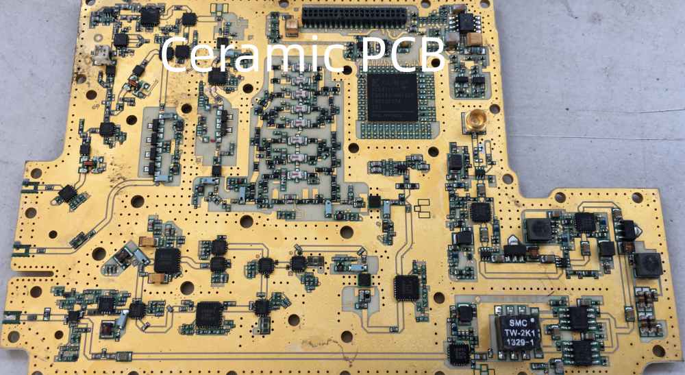
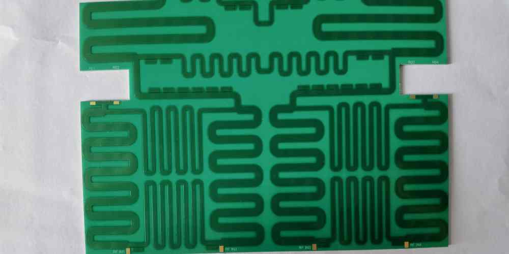
Ceramic printed circuit boards provide high reliability and performance making them ideal for demanding applications. However, fabrication of ceramic PCBs requires specialized processes that differ considerably from standard FR4 PCB manufacturing.
This article provides an overview of the key steps involved in making ceramic printed circuit boards.
Ceramic PCB Overview
Ceramic PCBs use ceramic materials like alumina or aluminum nitride as the insulating substrate instead of glass reinforced epoxy laminates used in FR4 PCBs.
Some properties of ceramic PCBs include:
- High heat tolerance exceeding 250°C
- Superior electrical insulation properties
- Improved thermal conductivity for heat dissipation
- Elimination of moisture absorption issues
- Hermetic sealing of components
- Better high frequency characteristics
These benefits make ceramic PCBs well-suited for automotive electronics, aerospace systems, military applications, power electronics and RF modules.
Ceramic PCB Manufacturing Process

The fabrication process for ceramic PCBs involves the following main steps:
Tape Casting
Ceramic powder is mixed with organic binders and cast onto a film carrier to produce thin flexible ceramic tapes, akin to creating green PCB prepregs.
Via Punching
Holes are mechanically punched through the ceramic tapes at locations requiring vertical interconnections between layers.
Conductor Printing
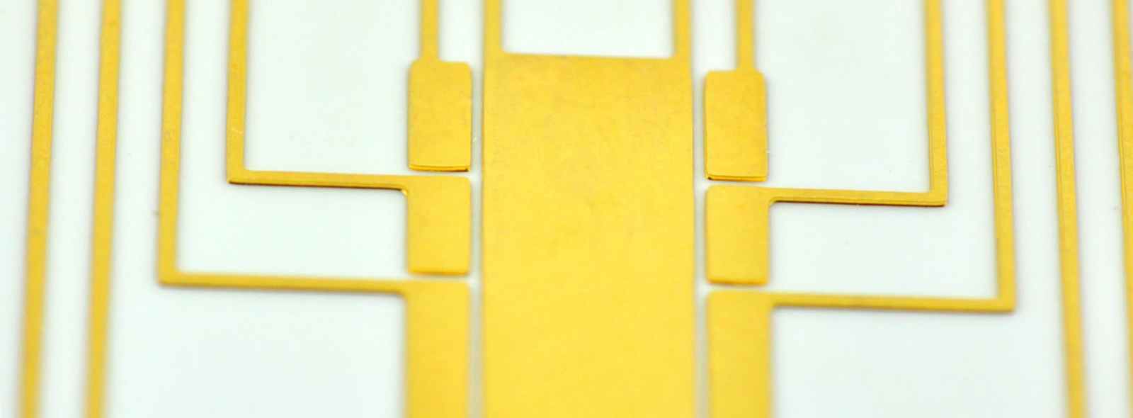
Conductive inks and pastes containing metallic particles like gold, silver or copper are screen printed onto the ceramic tapes to create the circuit traces and pads.
Sheet Cutting
The printed and punched ceramic tapes are precisely cut to the required board dimensions.
Layer Stacking
Cut ceramic layers with printed conductors are collated and stacked in the proper sequence using alignment fixtures. Stack may include plain dielectric layers also.
Lamination
The multilayer ceramic board stack undergoes heat and pressure to permanently bond the layers into a single rigid assembly.
Binder Burnout
The laminated board is slowly heated in a controlled profile to slowly decompose and drive off the organic binders from the ceramic material.
Sintering
The binder-free laminate undergoes firing at over 1000°C to densify and sinter the ceramic particles into a strong fused substrate with embedded conductors.
Edge Metallization
The fired ceramic board periphery is metallized to facilitate plated through hole formation and external wiring connections.
Via Hole Metallization
The fired through holes are activated and plated to form conductive interconnections between the layers.
Surface Finish
Immersion plating of gold, nickel or other finish is applied over the exposed conductors and vias to protect against oxidation and improve solderability.
Machining
Additional milling, drilling, grinding and cutting operations are done if necessary to achieve final board dimensions and hole locations.
Assembly
Components are finally soldered or epoxied onto the finished ceramic PCB using high temperature solders compatible with ceramics.
Key Differences from FR4 PCB Fabrication
Some of the major differences compared to standard FR4 PCB manufacturing are:
- Use of ceramic tapes instead of epoxy laminates
- Punching and printing of ceramic layers prior to lamination instead of drilling post-lamination
- Co-firing of metals and ceramics rather than panel plating
- High temperature sintering instead of lower temperature curing
- More challenging component assembly requiring high temperature solders
These differences allow ceramic PCBs to attain much higher temperature, power and frequency capabilities compared to organic FR4 boards.
Ceramic PCB Design Considerations

Some key design aspects that differ for ceramic PCBs include:
- Components require high temperature soldering or bonding techniques.
- Vias and traces have higher electrical resistance requiring compensation.
- Thermal expansion mismatches require analysis.
- Warpage control is critical since ceramics cannot tolerate much flexure.
- Panel sizes are smaller than FR4.
- Minimum feature sizes and spacing have tighter limits.
Advanced Ceramic PCB Technologies
Some advanced technologies being adopted for ceramic PCBs are:
Low Temperature Co-Fired Ceramics (LTCC)
Allows use of lower cost conductors by co-firing ceramics and metals at 850-1000°C instead of ~1600°C.
High Density Interconnect (HDI)
Incorporates finer line widths, laser micro-vias and stacked micro-vias to increase circuit density.
Embedded Passives
Burying passive components like resistors and capacitors within the ceramic PCB stackup rather than surface mounting.
Metal and Ceramic Composite
Combining ceramic dielectric layers with bonded metal plates of copper or aluminum to form complex hybrid substrates.
Direct Copper Bonding
Bonding a pure copper layer directly to the ceramic substrate for improved thermal conductivity.
Ceramic PCB Manufacturers
Some leading companies providing precision ceramic PCB fabrication include:
- Kyocera
- Maruwa
- Micro Systems Technologies (MST)
- Remtec
- Cicor Group
- ECRI Microelectronics
- Vijay Ceramics
- AMI Ceramics
These manufacturers can offer quick-turn prototyping to high volume production of ceramic printed circuit boards.
FAQs
What are ceramic PCBs used for?
Ceramic PCBs are typically used in high reliability applications like military, aerospace, automotive, medical, oil drilling, power electronics, RF modules etc. where high heat, frequency and power demands exist.
How to solder to ceramic PCB?
Active brazing alloys are often used to solder components to ceramic PCBs to withstand the high temperatures. Soldering steps may be done before firing or in post-fire surface mount.
Can you drill holes in ceramic PCB?
Yes, drilling is possible in fired ceramic PCBs using diamond-coated carbide bits. But holes are generally punched in ceramic layers before lamination to avoid surface cracking issues.
Are ceramic PCBs flexible?
No, ceramics are rigid and brittle, so ceramic PCBs cannot be flexed like FR4 PCBs. Some ultra-thin ceramic flex boards are under development but not in mainstream production.
Is ceramic PCB expensive?
Yes, ceramic PCBs typically cost at least 4-5 times more compared to FR4 PCBs mainly due to challenging fabrication process and smaller production volumes. Their high performance justifies the cost premium.
In summary, manufacturing ceramic PCBs requires specialized materials, processes and techniques tailored to the nature of ceramic materials. The complex fabrication is rewarded by the exceptional performance that ceramic printed circuit boards provide.


Leave a Reply