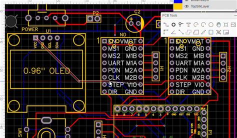
Introduction to High Current PCB Design
When designing printed circuit boards (PCBs) for high-current applications, several critical factors must be considered to ensure optimal performance, reliability, and safety. High-Current PCB design involves managing increased power demands, heat dissipation, and potential electromagnetic interference (EMI) issues. This comprehensive guide will delve into the essential aspects of high-current PCB design, providing insights and best practices for engineers and designers.
Understanding High Current PCB Applications
High-current PCBs find applications in various industries, including:
- Power electronics
- Automotive systems
- Industrial automation
- Telecommunications infrastructure
- Renewable energy systems
These applications often require the PCB to handle currents ranging from several amperes to hundreds of amperes, depending on the specific requirements of the system.
Key Considerations in High Current PCB Design
1. Trace Width and Thickness
One of the most critical aspects of high-current PCB design is determining the appropriate trace width and thickness. Traces must be wide enough to handle the required current without excessive heating or voltage drop. The IPC-2221 standard provides guidelines for calculating trace widths based on factors such as current, temperature rise, and copper thickness.
| Current (A) | Trace Width (mm) for 1 oz Copper | Trace Width (mm) for 2 oz Copper |
|---|---|---|
| 5 | 2.5 | 1.25 |
| 10 | 5.0 | 2.5 |
| 20 | 10.0 | 5.0 |
| 50 | 25.0 | 12.5 |
Table 1: Trace width recommendations for different current levels and copper thicknesses
2. Copper Weight and Thickness
The thickness of the copper layer on the PCB directly affects its current-carrying capacity. High-current PCBs often use thicker copper layers, such as 2 oz or 4 oz copper, to improve current handling and heat dissipation. However, thicker copper layers can increase manufacturing costs and make the PCB less flexible.
3. Thermal Management
High-current PCBs generate significant amounts of heat due to the increased power dissipation. Proper thermal management is essential to prevent component failure and ensure long-term reliability. Strategies for effective thermal management include:
- Using larger copper pours and planes to dissipate heat
- Incorporating thermal vias to transfer heat to other layers or heatsinks
- Selecting components with appropriate power ratings and thermal characteristics
- Employing active cooling methods, such as fans or liquid cooling, in extreme cases
4. Voltage Drop and Power Distribution
In high-current PCBs, voltage drop across traces can be a significant concern. Excessive voltage drop can lead to reduced performance and efficiency. To minimize voltage drop:
- Use wider traces and thicker copper layers to reduce resistance
- Keep high-current traces as short as possible
- Use dedicated power and Ground Planes for efficient power distribution
- Consider using voltage sense lines to compensate for voltage drop in critical circuits
5. EMI and Signal Integrity
High-current PCBs can be prone to electromagnetic interference (EMI) issues due to the large currents flowing through the traces. EMI can cause signal integrity problems and interfere with nearby electronic devices. To mitigate EMI:
- Keep high-current traces away from sensitive signals
- Use proper grounding techniques, such as a solid ground plane
- Implement shielding and filtering techniques, such as ferrite beads or EMI filters
- Follow best practices for layou


Leave a Reply