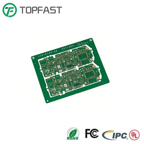
What is an HDI PCB?
High Density Interconnect (HDI) Printed Circuit Boards (PCBs) are advanced circuit boards that feature finer lines and spaces (<100 μm), smaller vias (<150 μm), and higher connection pad density than conventional PCBs. This enables HDI PCBs to pack a lot of functionality into a small form factor, making them ideal for compact and high-performance electronic devices such as smartphones, tablets, smartwatches, medical devices, and aerospace systems.
The main characteristics of HDI PCBs include:
– High density of interconnects
– Fine lines and spaces (typically less than 100 μm)
– Small vias (typically less than 150 μm)
– Thin copper and dielectric layers
– High layer counts (8 or more)
– Sequential lamination construction
– Microvias and buried/blind vias
Advantages of HDI PCBs
HDI PCBs offer several advantages over traditional PCBs:
-
Miniaturization: The high density of interconnects and use of microvias allows HDI PCBs to pack more functionality in a smaller size, enabling compact and lightweight product designs.
-
High Performance: The shorter signal paths and thinner dielectric layers in HDI PCBs result in faster signal speeds, lower noise, and better signal integrity compared to conventional PCBs.
-
Reliability: HDI PCBs use advanced manufacturing processes and materials that provide high reliability and durability, even under harsh operating conditions.
-
Cost Savings: Although HDI PCBs have a higher cost per unit area than conventional PCBs, they can often result in overall cost savings by reducing the number of layers, enabling smaller product size, and improving yield.

Challenges of HDI PCB Manufacturing
Despite their advantages, HDI PCBs also present some manufacturing challenges due to their high density and small features:
-
Precise Registration: The small features and tight tolerances in HDI PCBs require precise layer-to-layer registration during the lamination process to ensure proper alignment of vias and interconnects.
-
Drilling and Plating: The small vias in HDI PCBs require specialized drilling and plating equipment and processes to ensure proper formation and reliability.
-
Imaging and Etching: The fine lines and spaces in HDI PCBs require high-resolution imaging and precise etching control to achieve the desired feature sizes and avoid defects.
-
Impedance Control: The thin dielectric layers and close spacing of traces in HDI PCBs can make impedance control more challenging, requiring careful design and process control.
-
Testing and Inspection: The small features and high density of HDI PCBs can make visual inspection and electrical testing more difficult, often requiring specialized equipment and techniques.

How to Choose the Right HDI PCB Manufacturer
Choosing the right HDI PCB manufacturer is critical to ensuring the quality, reliability, and cost-effectiveness of your product. Here are some key factors to consider when selecting an HDI PCB manufacturer:
1. Technical Capabilities
Make sure the manufacturer has the necessary equipment, processes, and expertise to fabricate HDI PCBs with the features and specifications your design requires. Some key technical capabilities to look for include:
- Minimum line width and spacing (e.g. 50/50 μm or less)
- Minimum via size (e.g. 100 μm or less)
- Laser drilling and plasma etching capabilities
- Advanced lamination processes (e.g. MSAP, HDI, SLP)
- Copper filled microvias
- Impedance control
- Automated optical inspection (AOI) and electrical testing
2. Quality Management System
Choose a manufacturer that has a robust quality management system in place to ensure consistent and reliable HDI PCB Fabrication. Look for certifications such as:
- ISO 9001 Quality Management System
- IATF 16949 Automotive Quality Management System
- AS9100 Aerospace Quality Management System
- IPC-A-600 Acceptability of Printed Boards
- IPC Class 2 and Class 3 Capabilities
3. Experience and Track Record
HDI PCB manufacturing requires specialized knowledge and experience. Choose a manufacturer that has a proven track record of fabricating HDI PCBs for applications similar to yours. Ask for references, case studies, or sample boards to evaluate their experience and capabilities.
4. Capacity and Lead Times
Make sure the manufacturer has sufficient capacity to meet your production volume and lead time requirements. HDI PCBs often require longer fabrication times than conventional PCBs due to their complex processes. Get clear lead time estimates and confirm the manufacturer’s ability to scale up production as needed.
5. Customer Support and Communication
Good communication and customer support are essential for a successful HDI PCB manufacturing partnership. Choose a manufacturer that is responsive, proactive, and willing to work closely with you to address any issues or concerns. Consider factors such as:
- Ease of communication (e.g. language, time zone)
- Dedicated account manager or technical support
- Regular project updates and status reporting
- Flexibility to accommodate design changes or revisions
- Willingness to provide design for manufacturing (DFM) feedback
6. Cost and Value
While cost is an important consideration, it should not be the only factor in choosing an HDI PCB manufacturer. Look for a manufacturer that provides the best overall value in terms of quality, reliability, service, and price. Consider total cost of ownership (TCO) rather than just the unit price, taking into account factors such as:
- NRE (non-recurring engineering) costs
- Tooling and setup costs
- Minimum order quantity (MOQ) requirements
- Shipping and logistics costs
- Potential rework or scrap costs due to quality issues

Common HDI PCB Stackups and Technologies
HDI PCBs use various stackup and interconnect technologies to achieve high density and performance. Here are some common HDI PCB Stackups and their key features:
| Stackup | Layers | Interconnects | Features |
|---|---|---|---|
| 1+N+1 | 4-8 | Buried vias, blind vias, through-hole vias | Suitable for most HDI designs, cost-effective |
| 2+N+2 | 8-16 | Buried vias, blind vias, through-hole vias, staggered vias | Higher density and layer count than 1+N+1, allows staggered/stacked vias |
| 3+N+3 | 12-24 | Buried vias, blind vias, through-hole vias, staggered vias, HDI coreless | Highest density and layer count, uses coreless construction for thin profile and low warpage |
Some other HDI PCB technologies and processes include:
-
MSAP (Modified Semi-Additive Process): A manufacturing process that enables finer lines and spaces (down to 30 μm) by using a thin electroless copper seed layer and advanced etching techniques.
-
HDI Sequential Lamination: A fabrication process where HDI layers are built up sequentially and laminated together, allowing for buried and blind vias and higher layer counts.
-
Via-in-Pad: A design technique where vias are placed directly in component pads, allowing for higher density and smaller form factors.
-
Microvias: Small vias (typically <150 μm) that are used to interconnect HDI layers, enabling high-density designs and shorter signal paths.
FAQ
1. What is the difference between HDI PCBs and conventional PCBs?
HDI PCBs have higher interconnect density, finer lines and spaces, smaller vias, and thinner layers compared to conventional PCBs. This allows HDI PCBs to pack more functionality into a smaller form factor and achieve better electrical performance.
2. What are the main applications of HDI PCBs?
HDI PCBs are commonly used in compact and high-performance electronic devices such as smartphones, tablets, smartwatches, medical devices, aerospace systems, and advanced driver assistance systems (ADAS).
3. What are the typical layer counts and line widths/spaces in HDI PCBs?
HDI PCBs typically have 8 or more layers, with line widths and spaces less than 100 μm (3-4 mils). Some advanced HDI designs can have up to 24 layers and line widths/spaces down to 30 μm (1.2 mils).
4. How do HDI PCBs achieve higher density and performance compared to conventional PCBs?
HDI PCBs use advanced manufacturing processes such as MSAP, sequential lamination, and laser drilling to achieve finer features and higher interconnect density. They also use microvias, buried/blind vias, and via-in-pad design techniques to reduce signal path lengths and improve electrical performance.
5. What should I look for when choosing an HDI PCB manufacturer?
When choosing an HDI PCB manufacturer, consider factors such as technical capabilities, quality management system, experience and track record, capacity and lead times, customer support and communication, and overall cost and value. Make sure the manufacturer has the necessary expertise, equipment, and processes to fabricate HDI PCBs that meet your specific requirements and standards.


Leave a Reply