Copper Foil Definition
The copper foil definition in PCB engineering is straightforward: copper foil is a thin sheet of copper—typically 9 µm to 400 µm (roughly ¼ oz to 12 oz per square foot)—that serves as the conductive layer on a printed circuit board. It carries current, forms signal traces, and acts as the primary path for heat spreading. Understanding this copper foil definition is essential for selecting the right foil type and thickness for any board design.
On organic laminates such as FR-4, foil is laminated with adhesive or resin. On ceramic substrates, it is bonded through high-temperature processes such as direct bond copper (DBC) or active metal brazing (AMB), or deposited by sputtering and plating in direct plated copper (DPC) processes.
Electrodeposited vs. Rolled Annealed Foil
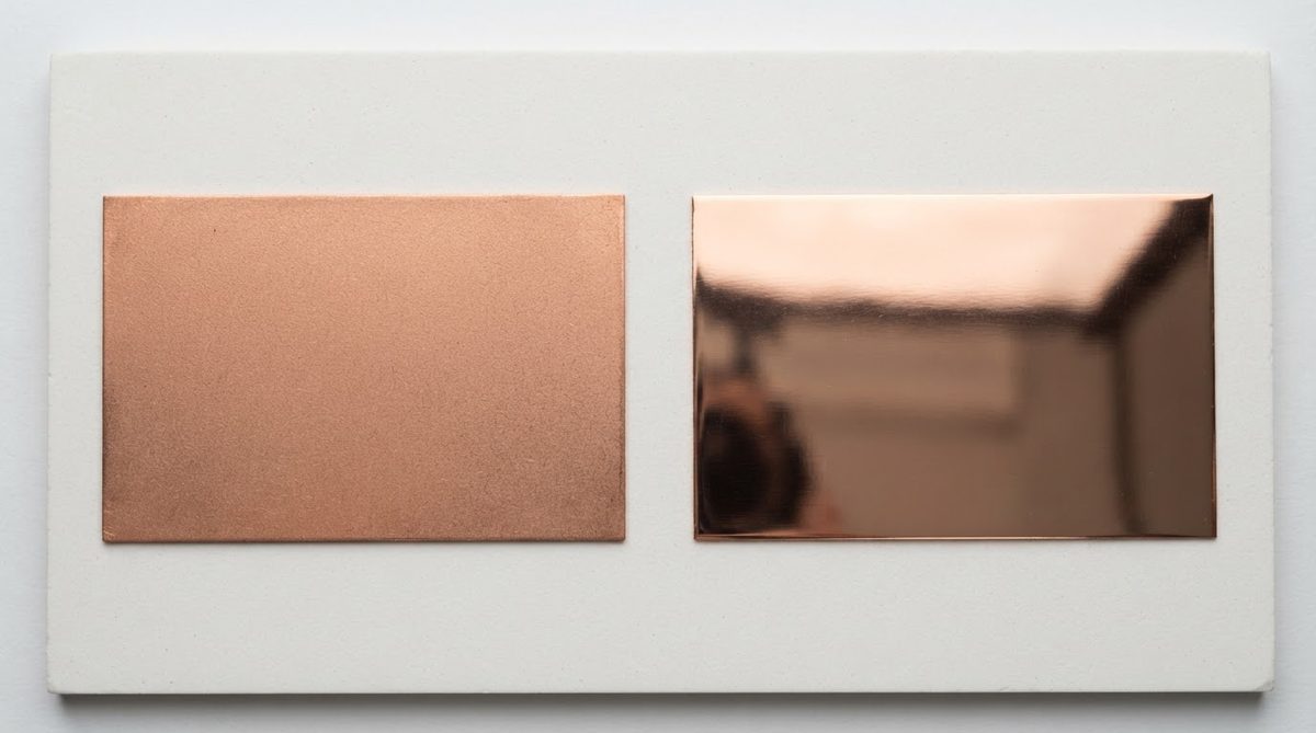
Two manufacturing methods produce nearly all PCB-grade copper foil. Knowing how each is made helps clarify which fits a given application, since the copper foil definition alone does not capture the performance differences between them.
Electrodeposited (ED) foil is plated onto a rotating titanium drum from a copper sulfate bath. One side is matte and rough, which improves adhesion to substrates. Rolled annealed (RA) foil is mechanically rolled from a copper ingot and then annealed. RA foil is smoother on both sides, more ductile, and better suited to flex circuits or high-frequency applications where surface roughness increases conductor loss.
Key differences at a glance:
- Surface roughness: ED foil has a rough matte side (Rz 3–8 µm typical); RA foil is smooth on both sides (Rz < 1.5 µm).
- Ductility: RA foil withstands repeated bending, making it the standard choice for flex and rigid-flex circuits.
- Adhesion: The rough side of ED foil bonds more readily to resin and ceramic surfaces without extra surface treatment.
- Signal integrity: At frequencies above roughly 5 GHz, the smoother profile of RA foil reduces skin-effect losses measurably.
Common Thickness Grades
| Weight designation | Nominal thickness (µm) | Typical use |
|---|---|---|
| ¼ oz | 9 | Fine-line HDI, RF traces |
| ½ oz | 18 | Signal layers, low-current digital |
| 1 oz | 35 | General-purpose, most prototypes |
| 2 oz | 70 | Power distribution, high-current paths |
| 3 oz | 105 | Power electronics, bus bars |
| 6–12 oz | 210–400 | Heavy-copper power modules |
Weight designations follow IPC-4562A. One ounce refers to one ounce of copper spread over one square foot, yielding approximately 35 µm of thickness. When engineers reference the copper foil definition in procurement documents, they almost always specify foil by this weight-per-area convention rather than by raw thickness.
How Copper Foil Bonds to Ceramic Substrates
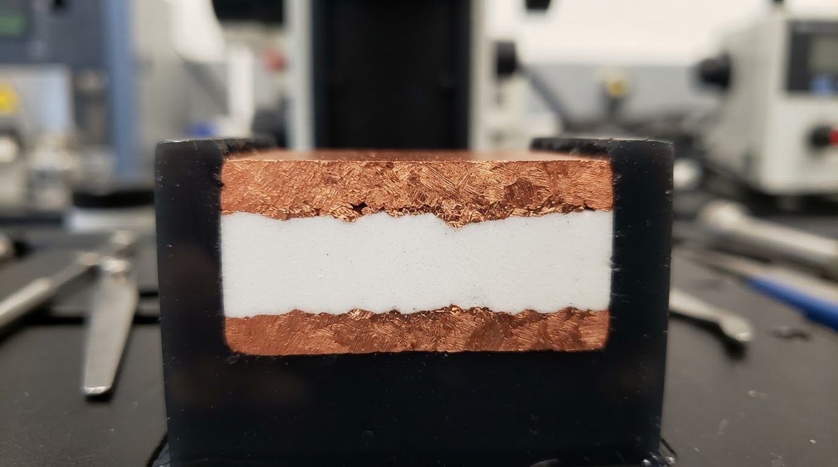
Bonding copper foil to a ceramic substrate demands different techniques than organic lamination. In DBC, a copper sheet is oxidised at its surface and then heated to roughly 1 065 °C so the copper-oxide eutectic wets the alumina or aluminium nitride surface. The result is a direct metallurgical bond with no adhesive layer, which gives excellent thermal conductivity through the joint. AMB uses a reactive braze alloy (commonly AgCuTi) to bond thicker copper sheets—up to 800 µm—to silicon nitride or AlN substrates for high-reliability power modules.
Because ceramic and copper have different coefficients of thermal expansion (CTE), foil thickness on ceramic boards must be balanced: thicker copper carries more current and spreads heat better, but it also increases thermomechanical stress during temperature cycling. Power-module designers typically run thermal-cycling simulations before committing to a copper thickness above 300 µm on AlN or Si₃N₄ substrates.
FAQ
Is copper foil the same as copper cladding?
In PCB terminology, yes. “Copper-clad” means a substrate with copper foil already bonded to one or both sides. The foil itself is the cladding, so the copper foil definition covers both terms.
Does foil purity matter for PCBs?
Standard ED foil is ≥ 99.8 % copper per IPC-4562A. For most digital and power applications this is sufficient. High-frequency or cryogenic designs sometimes specify oxygen-free high-conductivity (OFHC) copper at ≥ 99.99 % purity to minimise resistive loss.
Can I use any copper thickness on a ceramic PCB?
Not freely. DBC typically supports 127–500 µm copper; DPC supports thinner layers, often 1–100 µm built up by sputtering and electroplating. The ceramic material and its CTE mismatch with copper set the practical upper limit before delamination risk becomes unacceptable.