Introduction to Multi-layer PCBs
Multi-layer printed circuit boards (PCBs) have revolutionized the electronics industry by enabling the design and manufacture of compact, high-performance electronic devices. These complex boards consist of multiple layers of conductive and insulating materials, allowing for increased circuit density and improved signal integrity. In this article, we will explore the world of multi-layer PCBs, discussing their structure, manufacturing process, advantages, and applications.
What are Multi-layer PCBs?
Multi-layer PCBs are printed circuit boards that consist of three or more conductive layers, separated by insulating layers. The conductive layers are typically made of copper, while the insulating layers are made of materials such as FR-4, a glass-reinforced epoxy laminate. The layers are bonded together using heat and pressure, forming a single, cohesive board.
Advantages of Multi-layer PCBs
- Increased circuit density
- Improved signal integrity
- Reduced electromagnetic interference (EMI)
- Enhanced thermal management
- Reduced board size and weight
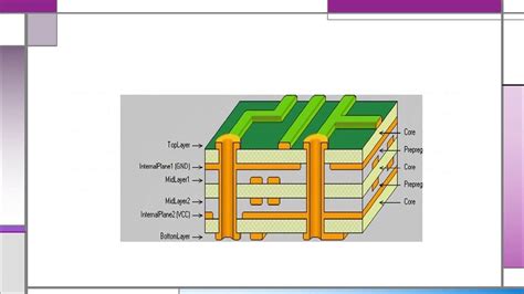
Structure of Multi-layer PCBs
Layers in a Multi-layer PCB
A multi-layer PCB consists of several distinct layers, each serving a specific purpose. The most common layers found in a multi-layer PCB include:
- Signal layers: These layers contain the actual circuit traces that carry electrical signals between components.
- Power and ground planes: These layers provide a stable reference voltage and help to reduce EMI.
- Insulating layers: These layers, made of materials like FR-4, separate the conductive layers and provide electrical isolation.
Layer Stackup
The arrangement of layers in a multi-layer PCB is known as the layer stackup. The stackup is designed to optimize signal integrity, minimize EMI, and ensure proper functionality of the circuit. A typical 4-layer PCB stackup might consist of the following layers:
| Layer | Description |
|---|---|
| Top | Signal layer |
| Inner 1 | Ground plane |
| Inner 2 | Power plane |
| Bottom | Signal layer |
Via Types
Vias are conductive pathways that connect different layers of a multi-layer PCB. There are several types of vias used in multi-layer PCBs:
- Through-hole vias: These vias pass through all layers of the board and are typically used for component mounting.
- Blind vias: These vias connect an outer layer to an inner layer, but do not pass through the entire board.
- Buried vias: These vias connect inner layers without reaching the outer layers of the board.

Manufacturing Process of Multi-layer PCBs
PCB Design and Layout
The first step in manufacturing a multi-layer PCB is designing the circuit and creating the PCB layout. This involves using specialized software to create a schematic diagram of the circuit and then translating that schematic into a physical layout of the board. The layout must take into account factors such as signal integrity, EMI, and thermal management.
Layer Fabrication
Once the layout is finalized, the individual layers of the PCB are fabricated. This typically involves the following steps:
- Applying a photoresist coating to the copper-clad laminate
- Exposing the photoresist to UV light through a photomask
- Developing the photoresist to remove the unexposed areas
- Etching away the unwanted copper
- Stripping the remaining photoresist
Lamination and Drilling
After the individual layers are fabricated, they are stacked and aligned according to the layer stackup. The layers are then bonded together using heat and pressure in a process called lamination. Once laminated, the board is drilled to create the necessary vias and component mounting holes.
Plating and Finishing
The drilled holes are then plated with copper to create conductive pathways between layers. Additional surface finishes, such as solder mask and silkscreen, are applied to protect the board and aid in component assembly.

Advantages of Multi-layer PCBs
Increased Circuit Density
One of the primary advantages of multi-layer PCBs is their ability to accommodate high circuit densities. By utilizing multiple layers, designers can route a large number of signals in a relatively small area. This allows for the creation of compact, high-performance electronic devices.
Improved Signal Integrity
Multi-layer PCBs offer improved signal integrity compared to single or double-layer boards. By using dedicated power and ground planes, designers can minimize signal noise and ensure stable reference voltages. Additionally, the use of controlled impedance traces and careful layer stackup design can help to reduce signal reflections and crosstalk.
Reduced Electromagnetic Interference (EMI)
The use of power and ground planes in multi-layer PCBs helps to reduce electromagnetic interference (EMI). These planes act as shields, containing electromagnetic fields generated by the signals on the board. This shielding effect minimizes the amount of EMI radiated by the board, which is particularly important in sensitive electronic devices.
Enhanced Thermal Management
Multi-layer PCBs can be designed with dedicated layers for thermal management. These layers, often made of materials with high thermal conductivity, help to spread heat evenly across the board and away from temperature-sensitive components. This improves the overall reliability and longevity of the electronic device.
Reduced Board Size and Weight
By accommodating high circuit densities, multi-layer PCBs enable the design of smaller and lighter electronic devices. This is particularly important in applications where space and weight are critical factors, such as in aerospace and portable electronics.

Applications of Multi-layer PCBs
Multi-layer PCBs are used in a wide range of industries and applications, including:
- Consumer electronics (smartphones, tablets, laptops)
- Automotive electronics (infotainment systems, engine control units)
- Medical devices (imaging equipment, patient monitors)
- Aerospace and defense (avionics, radar systems)
- Industrial automation (process controllers, sensors)
Frequently Asked Questions (FAQ)
1. What is the difference between a multi-layer PCB and a single-layer PCB?
A single-layer PCB consists of a single conductive layer, while a multi-layer PCB has three or more conductive layers separated by insulating layers. Multi-layer PCBs offer higher circuit density, improved signal integrity, and better EMI performance compared to single-layer boards.
2. How many layers can a multi-layer PCB have?
Multi-layer PCBs can have anywhere from 3 to over 50 layers, depending on the complexity of the circuit and the application requirements. Most common multi-layer PCBs have 4, 6, 8, or 10 layers.
3. What materials are used in the construction of multi-layer PCBs?
The conductive layers in a multi-layer PCB are typically made of copper, while the insulating layers are made of materials such as FR-4, a glass-reinforced epoxy laminate. Other materials, such as polyimide or PTFE, may be used for high-frequency or high-temperature applications.
4. How does the manufacturing process differ for multi-layer PCBs compared to single-layer PCBs?
The manufacturing process for multi-layer PCBs is more complex than that of single-layer PCBs. It involves fabricating individual layers, aligning and laminating them together, drilling vias, and plating the holes to create conductive pathways between layers. Single-layer PCBs do not require lamination or drilling of vias.
5. What are the main advantages of using multi-layer PCBs in electronic devices?
The main advantages of using multi-layer PCBs include increased circuit density, improved signal integrity, reduced electromagnetic interference (EMI), enhanced thermal management, and reduced board size and weight. These advantages enable the design of compact, high-performance electronic devices.
Conclusion
Multi-layer PCBs have become an essential component in the design and manufacture of modern electronic devices. By offering increased circuit density, improved signal integrity, and reduced EMI, these complex boards enable the creation of compact, high-performance electronics across a wide range of industries. As electronic systems continue to advance, the demand for multi-layer PCBs with even higher layer counts and more advanced features is expected to grow. Understanding the structure, manufacturing process, and advantages of multi-layer PCBs is crucial for engineers, designers, and manufacturers looking to stay at the forefront of the electronics industry.


Leave a Reply