Understanding Differential Trace Impedance
Differential trace impedance is a critical aspect of High-Speed PCB design, especially when dealing with differential signaling. It refers to the impedance between two differential traces, which carry equal and opposite signals. Maintaining a consistent differential impedance is essential for preserving signal integrity and minimizing electromagnetic interference (EMI).
What is Differential Signaling?
Differential signaling is a technique used in high-speed digital communication where two complementary signals are transmitted over a pair of conductors. The signal is represented by the voltage difference between the two conductors, rather than the absolute voltage level with respect to ground. This approach offers several advantages, such as:
- Improved noise immunity
- Reduced electromagnetic interference (EMI)
- Higher data rates
- Better power efficiency
The Role of Impedance Matching
In order to ensure proper signal transmission and minimize reflections, it is crucial to match the impedance of the differential traces to the characteristic impedance of the transmitter and receiver. Impedance mismatches can lead to signal distortion, reduced signal integrity, and increased EMI.
The characteristic impedance of a differential pair is determined by several factors, including:
- Trace width and spacing
- Dielectric constant of the PCB material
- Thickness of the PCB
- Presence of a reference plane
Challenges of Differential Trace Impedance Without Reference Plane
Designing differential traces without a reference plane presents unique challenges in maintaining consistent impedance. A reference plane, such as a ground or power plane, plays a crucial role in controlling the impedance of the traces by providing a low-impedance return path for the signals.
Impact on Impedance Control
Without a reference plane, the impedance of the differential traces becomes more sensitive to variations in the PCB Stackup and the surrounding environment. This can lead to impedance mismatches and signal integrity issues.
The absence of a reference plane also makes it more difficult to calculate and simulate the impedance of the differential traces accurately. Traditional impedance calculation methods, such as the microstrip or stripline formulas, assume the presence of a reference plane.
Increased Electromagnetic Interference (EMI)
Differential traces without a reference plane are more susceptible to EMI, both in terms of emission and susceptibility. The lack of a low-impedance return path can cause the signals to radiate more energy, leading to increased EMI emissions.
Furthermore, the absence of a reference plane makes the differential traces more vulnerable to external electromagnetic fields, which can couple into the traces and cause signal integrity issues.

Strategies for Managing Differential Trace Impedance Without Reference Plane
Despite the challenges, there are several strategies that can be employed to manage differential trace impedance in the absence of a reference plane. These strategies aim to minimize the impact of impedance variations and reduce EMI.
1. Careful PCB Stackup Design
A well-designed PCB stackup is crucial for maintaining consistent differential impedance without a reference plane. Consider the following guidelines:
- Use symmetrical stackups to minimize the impact of variations in dielectric constant and thickness.
- Minimize the distance between the differential traces and the nearest reference plane, if present in other layers.
- Choose PCB Materials with stable dielectric constants and low loss tangents.
2. Trace Geometry Optimization
Optimizing the geometry of the differential traces can help control impedance and reduce EMI. Consider the following techniques:
- Adjust trace width and spacing to achieve the desired impedance.
- Use serpentine routing or zig-zag patterns to minimize the loop area and reduce EMI.
- Implement guard traces or coplanar waveguides to provide shielding and improve impedance control.
3. Differential Impedance Simulation and Modeling
Advanced PCB design tools offer differential impedance simulation and modeling capabilities that can help optimize trace geometry and predict impedance behavior in the absence of a reference plane. These tools take into account the complex interactions between the traces, dielectrics, and surrounding structures.
By simulating and modeling the differential impedance, designers can identify potential issues early in the design process and make necessary adjustments to ensure consistent impedance and minimize EMI.
4. Experimental Validation and Tuning
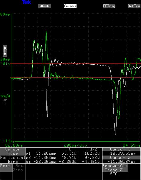
Despite careful design and simulation, it is essential to validate the differential impedance through experimental measurements. Time-domain reflectometry (TDR) and vector network analyzer (VNA) measurements can provide valuable insights into the actual impedance profile of the differential traces.
Based on the measurement results, designers can fine-tune the trace geometry, adjust the PCB stackup, or implement additional EMI mitigation techniques to achieve the desired impedance and signal integrity.

Real-World Applications and Case Studies
Differential trace impedance control without a reference plane is relevant in various high-speed digital applications, such as:
- High-speed serial interfaces (e.g., USB, PCIe, SATA)
- Gigabit Ethernet and 10 Gigabit Ethernet
- LVDS (Low-Voltage Differential Signaling) interfaces
- HDMI and DisplayPort
Case Study 1: USB 3.0 Differential Pair Routing
In a USB 3.0 design, a differential pair was routed on an outer layer without a reference plane. To maintain consistent impedance and minimize EMI, the following strategies were employed:
- The trace width and spacing were optimized based on the PCB stackup and dielectric properties.
- Guard traces were placed adjacent to the differential pair to provide shielding and improve impedance control.
- Serpentine routing was used to minimize the loop area and reduce EMI.
Through careful design and simulation, the differential impedance was maintained within the specified tolerance, and the USB 3.0 interface functioned reliably.
Case Study 2: High-Speed DDR Memory Interface
In a high-speed DDR memory interface design, differential traces were routed on an inner layer without a dedicated reference plane. To ensure signal integrity and minimize crosstalk, the following techniques were applied:
- The PCB stackup was optimized to minimize the distance between the differential traces and the nearest reference plane.
- Coplanar waveguides were implemented to provide shielding and improve impedance control.
- Extensive simulation and modeling were performed to optimize the trace geometry and predict the impedance behavior.
Experimental measurements confirmed that the differential impedance was well-controlled, and the DDR memory interface operated at the desired data rates with minimal signal distortion.

Frequently Asked Questions (FAQ)
1. What is the impact of not having a reference plane on differential trace impedance?
Without a reference plane, the impedance of differential traces becomes more sensitive to variations in the PCB stackup and the surrounding environment. This can lead to impedance mismatches, increased EMI, and signal integrity issues.
2. How can I calculate differential impedance without a reference plane?
Calculating differential impedance without a reference plane is more complex than traditional methods that assume the presence of a reference plane. Advanced PCB design tools with differential impedance simulation and modeling capabilities can help predict the impedance behavior in the absence of a reference plane.
3. What are some strategies for controlling differential impedance without a reference plane?
Strategies for controlling differential impedance without a reference plane include careful PCB stackup design, trace geometry optimization (e.g., adjusting width and spacing, using serpentine routing or coplanar waveguides), differential impedance simulation and modeling, and experimental validation and tuning.
4. How does the absence of a reference plane affect EMI?
Differential traces without a reference plane are more susceptible to EMI, both in terms of emission and susceptibility. The lack of a low-impedance return path can cause the signals to radiate more energy, leading to increased EMI emissions. The traces are also more vulnerable to external electromagnetic fields, which can couple into the traces and cause signal integrity issues.
5. Can I achieve reliable high-speed performance without a reference plane for differential traces?
While it is more challenging to achieve reliable high-speed performance without a reference plane for differential traces, it is possible with careful design, simulation, and validation. By employing strategies such as optimizing PCB stackup, trace geometry, and using advanced simulation tools, designers can control differential impedance and ensure signal integrity in the absence of a reference plane.
Conclusion
Designing differential traces without a reference plane presents unique challenges in maintaining consistent impedance and ensuring signal integrity. The absence of a low-impedance return path makes the differential traces more sensitive to variations in the PCB stackup and increases their susceptibility to EMI.
To overcome these challenges, designers must employ a combination of strategies, including careful PCB stackup design, trace geometry optimization, differential impedance simulation and modeling, and experimental validation and tuning. By understanding the impact of not having a reference plane and applying appropriate design techniques, it is possible to achieve reliable high-speed performance in differential signaling applications.
As high-speed digital systems continue to push the boundaries of data rates and signal integrity, the ability to control differential trace impedance without a reference plane becomes increasingly important. With the right tools, knowledge, and design practices, engineers can successfully tackle this challenge and develop robust and reliable high-speed PCB designs.


Leave a Reply