Blog
-
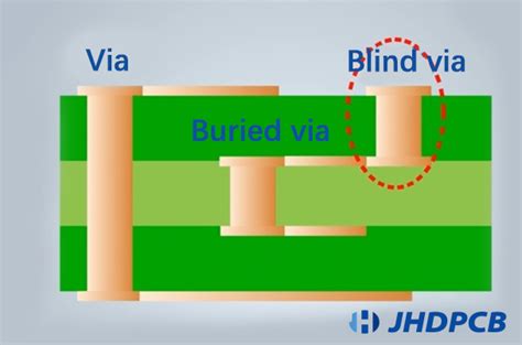
Blind and Buried Vias
Posted by
–
Read more: Blind and Buried ViasWhat are Blind Vias? Blind vias are a type of interconnect used in printed circuit boards (PCBs) that start on an outer layer and terminate on an inner layer, without going through the entire thickness of the board. Unlike Through-Hole Vias, which penetrate all layers of the PCB, blind vias […]
-
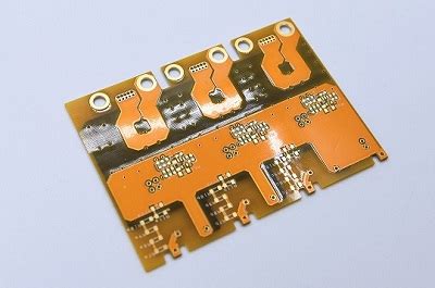
Innerlayer imaging for multilayer PCB
Posted by
–
 Read more: Innerlayer imaging for multilayer PCB
Introduction to Innerlayer imaging Innerlayer imaging is a crucial process in the manufacturing of multilayer printed circuit boards (PCBs). It involves transferring the circuit pattern onto the copper-clad laminate, which will be used as an inner layer in the final PCB Stack-Up. The accuracy and precision of innerlayer imaging directly […]
-
Gross PCB Material Price
Posted by
–
 Read more: Gross PCB Material Price
Introduction to PCB Material Pricing Printed Circuit Boards (PCBs) are essential components in modern electronics, forming the backbone of devices ranging from smartphones to aerospace systems. The cost of manufacturing PCBs is heavily influenced by the materials used in their construction. This comprehensive guide will delve into the various aspects […]
-
PCB services based on material choice
Posted by
–
 Read more: PCB services based on material choice
Introduction to PCB Material Selection Printed Circuit Boards (PCBs) are the backbone of modern electronics, providing a platform for interconnecting and mounting electronic components. The choice of materials used in PCB fabrication plays a crucial role in determining the performance, reliability, and cost of the final product. PCB Services offer […]
-
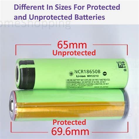 Read more: 18650 Battery Specifications – Essential for Implementing Any Technical Design
What are 18650 Batteries? 18650 batteries are rechargeable lithium-ion cells that derive their name from their physical dimensions: 18mm in diameter and 65mm in length. These cells have gained popularity due to their high energy density, long lifespan, and versatile applications. They are commonly used in consumer electronics, power tools, […]
-
Hex Inverter – 3 Main Types of Hex Inverter ICs
Posted by
–
 Read more: Hex Inverter – 3 Main Types of Hex Inverter ICs
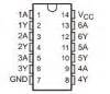
Introduction to Hex Inverters Hex inverters are digital logic gates that perform the logical NOT operation on six independent inputs simultaneously. These integrated circuits (ICs) are widely used in various electronic applications, such as signal conditioning, data processing, and digital system design. Hex inverters offer a compact and efficient solution […]
-
PCB Connector Types – What You Need To Know
Posted by
–
 Read more: PCB Connector Types – What You Need To Know
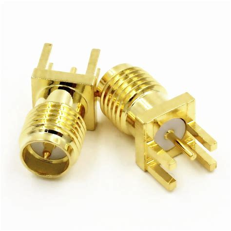
What are PCB Connectors? PCB connectors, short for printed circuit board connectors, are electrical components that facilitate the connection between two or more printed circuit boards or between a PCB and other components such as cables, wires, or devices. These connectors ensure reliable electrical and mechanical connections, allowing for the […]
-
Thick copper PCBs
Posted by
–
 Read more: Thick copper PCBs
Introduction to Copper PCBs Printed Circuit Boards (PCBs) are the backbone of modern electronics. They provide a platform for electrical components to be mounted and interconnected, enabling the creation of complex circuits and systems. One crucial aspect of PCB design is the choice of materials, particularly the copper layer thickness. […]
-
 Read more: Altium Polygon pour breaks on rigid flex split lines
Introduction to Polygon pours in Altium Designer Polygon pours are a powerful feature in Altium Designer that allow you to fill large areas of your PCB with copper. They are commonly used for power and ground planes, shielding, and creating custom copper shapes. However, when working with Rigid-Flex Designs, polygon […]
-
PCB design of DFM some matters needing attention
Posted by
–
 Read more: PCB design of DFM some matters needing attention
What is DFM in PCB Design? DFM (Design for Manufacturability) is the process of proactively designing products to optimize all manufacturing functions – fabrication, assembly, test, procurement, shipping, delivery, service, and repair. The goal is to achieve the lowest possible total cost while maintaining the required quality and reliability. In […]


