Blog
-
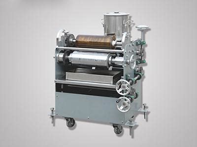
Read more: Curtain Coating – High-Speed with Low Material Loss LPI Applying Method
What is Curtain Coating? Curtain coating is a high-speed, non-contact coating method used to apply a thin, uniform layer of liquid onto a moving substrate. In this process, a continuous curtain of coating liquid freely falls onto the substrate which is moving underneath the curtain. As the substrate passes through […]
-
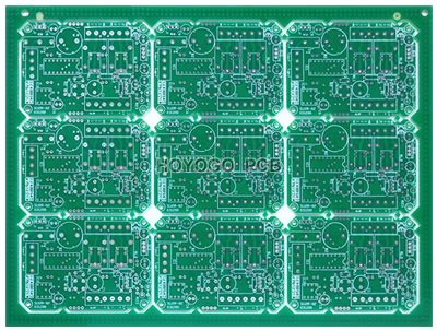
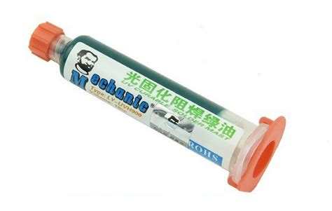
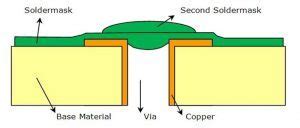
What is Peelable Soldermask?
Posted by
–
 Read more: What is Peelable Soldermask?
How Peelable Soldermask Works Peelable soldermask is typically applied to PCBs using screen printing or spray coating techniques. The mask is composed of a polymer material that is formulated to withstand the high temperatures associated with soldering while remaining easy to remove once the process is complete. The main functions […]
-
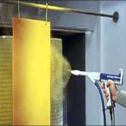
What Is The Typical Powder Spray Process?
Posted by
–
 Read more: What Is The Typical Powder Spray Process?
Understanding the Powder Spray Process The powder spray process consists of several key steps that ensure the proper application and adhesion of the coating material to the surface. These steps include: Surface Preparation Powder Application Curing Surface Preparation Before the powder coating can be applied, the surface of the object […]
-
 Read more: Advantages and Disadvantages of Electrostatic Powder Spray
Introduction to Electrostatic Powder Spray Electrostatic powder spray is a coating process that uses electrically charged particles to create a uniform and durable finish on various surfaces. This technology has gained popularity in recent years due to its numerous benefits, including improved efficiency, reduced waste, and enhanced coating quality. In […]
-
Red Solder Resist is Eye-catching
Posted by
–
 Read more: Red Solder Resist is Eye-catching
Introduction to Eye-catching Red Solder Resist Solder resist, also known as solder mask, is a protective coating applied to printed circuit boards (PCBs) to prevent solder bridges and short circuits during the soldering process. While green is the most common color for solder resist, red has become increasingly popular due […]
-
 Read more: What are the differences between solder mask and paste mask?
Introduction to Solder Paste Mask Solder paste mask, also known as solder mask or solder resist, is a protective layer applied to printed circuit boards (PCBs) during the manufacturing process. Its primary purpose is to prevent solder from adhering to unwanted areas of the PCB, ensuring that the solder only […]
-
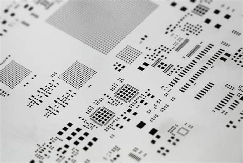
What is a PCB Stencil?
Posted by
–
 Read more: What is a PCB Stencil?
How PCB Stencils Work PCB stencils work by providing a uniform layer of solder paste on the PCB pads. The stencil is placed on top of the PCB, and solder paste is spread across the stencil using a squeegee. The solder paste passes through the openings in the stencil and […]
-
How to Generate AD Files Into Gerber
Posted by
–
 Read more: How to Generate AD Files Into Gerber
What is a Gerber File? Gerber files, also known as Gerber image or Gerber format files, contain the essential information needed to manufacture a printed circuit board (PCB). They are generated from PCB design software like Altium Designer and sent to PCB fabricators. A complete Gerber file package includes: Copper […]
-
Reasons of Solder Mask Bridge Breaking Off
Posted by
–
 Read more: Reasons of Solder Mask Bridge Breaking Off
Introduction to Solder Mask Bridges A solder mask bridge is a thin layer of solder mask material that spans across two or more adjacent pads or traces on a printed circuit board (PCB). The purpose of the solder mask bridge is to prevent solder from flowing between the pads during […]
-
What is solder mask dam?
Posted by
–
 Read more: What is solder mask dam?
Introduction to Solder Mask Dam Solder mask dam is an important feature in printed circuit board (PCB) design and manufacturing. It involves creating a barrier or “dam” around specific areas of the PCB using solder mask material. The purpose of solder mask dam is to contain the flow of liquid […]


