
Blog
-
PCB Design Companies in China
Posted by
–
 Read more: PCB Design Companies in China
Why Choose PCB Design Companies in China? There are several reasons why businesses choose to work with PCB design companies in China: Cost-effectiveness: China’s lower labor costs and efficient manufacturing processes allow for competitive pricing on PCB design and fabrication services. Expertise: Many Chinese PCB design companies have years of […]
-
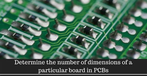 Read more: Top factors that determine the cost of Multilayer PCB Assembly!
Introduction to Multilayer PCB Assembly and Its Costs Printed Circuit Board (PCB) assembly is a crucial process in the manufacturing of electronic devices. It involves soldering electronic components onto a PCB to create a functional circuit. Multilayer PCBs, which consist of multiple layers of conductive material separated by insulating layers, […]
-
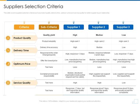 Read more: Top Factors to Consider for Selection of PCB Supplier!
Understanding the Role of PCBs in Electronics Manufacturing Before diving into the selection criteria for PCB suppliers, it’s essential to understand the importance of PCBs in electronics manufacturing. PCBs are the backbone of modern electronic devices, providing a platform for components to be mounted and interconnected. They play a vital […]
-
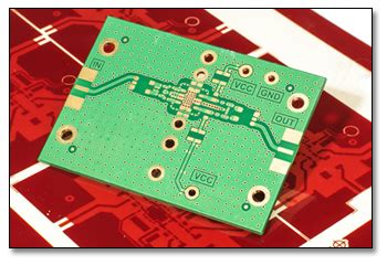 Read more: Build a New Product quickly with PCB Assembly Prototyping – A Brief Guide!
Introduction to PCB prototyping PCB (Printed Circuit Board) prototyping is a crucial step in the development of new electronic products. It allows engineers and designers to test and refine their designs before committing to full-scale production. In this article, we will explore the process of PCB prototyping, its benefits, and […]
-
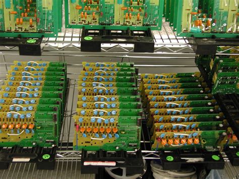 Read more: Do you ofer ROHS complint PCB asmbiles and potoypes?
What is RoHS Compliance? The RoHS directive, first introduced by the European Union (EU) in 2002 and later revised in 2011 (RoHS 2) and 2015 (RoHS 3), restricts the use of six hazardous substances in electronic and electrical equipment: Lead (Pb) Mercury (Hg) Cadmium (Cd) Hexavalent Chromium (Cr6+) Polybrominated Biphenyls […]
-
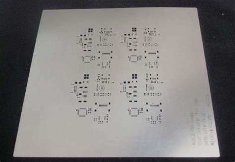 Read more: How and Why the utilization of SMT stencils simplify the Process of PCB Prototyping?
Introduction to SMT Stencils and PCB prototyping Printed circuit board (PCB) prototyping is an essential step in the development of electronic products. It allows engineers to test and validate their designs before moving to mass production. However, the process of PCB prototyping can be complex and time-consuming, especially when it […]
-
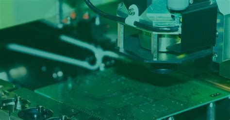 Read more: Top Factors to Consider While Outsourcing the Box Build PCB Assembly!
Introduction When it comes to manufacturing electronic devices, outsourcing the box build PCB assembly can be a cost-effective and efficient solution. However, choosing the right PCB Outsourcing partner is crucial to ensure the success of your project. In this article, we will discuss the top factors to consider while outsourcing […]
-
Why Opt for Outsourcing PCB Design Services?
Posted by
–
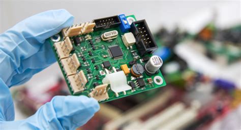 Read more: Why Opt for Outsourcing PCB Design Services?
Introduction Printed Circuit Boards (PCBs) are essential components of modern electronic devices. They provide the foundation for electrical connections and enable the functioning of complex systems. As technology advances and consumer demands evolve, the need for high-quality and efficient PCB design services has become more critical than ever. In this […]
-
What is a Blind Via?
Posted by
–
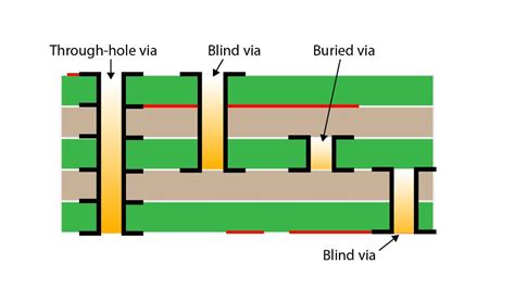 Read more: What is a Blind Via?
Introduction to Blind Vias In the world of printed circuit board (PCB) design, vias play a crucial role in interconnecting different layers of a multi-layer PCB. Among the various types of vias, blind vias have gained significant importance due to their ability to optimize board space and improve signal integrity. […]
-
Immersion Tin (ImSn) PCB Finish
Posted by
–
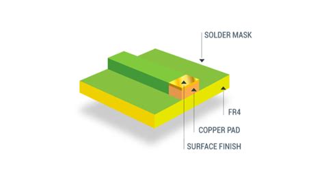 Read more: Immersion Tin (ImSn) PCB Finish
Introduction to Immersion Tin (ImSn) PCB Finish Immersion Tin (ImSn) is a popular surface finish for printed circuit boards (PCBs) in the electronics industry. This finish provides excellent solderability, flatness, and environmental compatibility, making it a preferred choice for many applications. ImSn is a lead-free finish that complies with RoHS […]


