Blog
-
 Read more: Top Design Guidelines for RF and Microwave PCB Assembly!
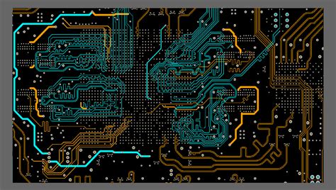
Introduction to PCB Design for RF and Microwave Applications Printed circuit board (PCB) design plays a critical role in the performance of radio frequency (RF) and microwave electronics. At these high frequencies, the PCB substrate materials, layout, and assembly techniques can significantly impact signal integrity, power efficiency, noise, and reliability. […]
-
5 tips for PCB schematic file management
Posted by
–
 Read more: 5 tips for PCB schematic file management
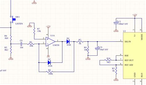
1. Use a Consistent File Naming Convention Establishing and adhering to a standardized file naming system is crucial for keeping your PCB Schematic files organized and easily identifiable. Consider including the following elements in your file names: Project or product name PCB version number Design revision or date Designer initials […]
-
Ten Common problems in PCB Design
Posted by
–
 Read more: Ten Common problems in PCB Design
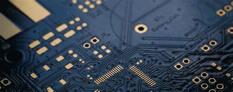
Introduction Printed Circuit Board (PCB) design is a crucial aspect of electronic product development. It involves the creation of a layout that connects electronic components to form a functional circuit. However, PCB Design is not without its challenges. In this article, we will discuss ten common problems encountered in PCB […]
-
 Read more: Introduction to PCB design of impedance matching with zero resistance
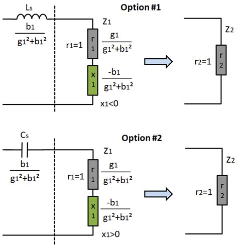
Understanding Impedance Matching What is Impedance? Impedance is a measure of the opposition that a circuit presents to a current when a voltage is applied. It is a complex quantity that consists of both resistance and reactance. In PCB Design, impedance plays a vital role in determining how signals propagate […]
-
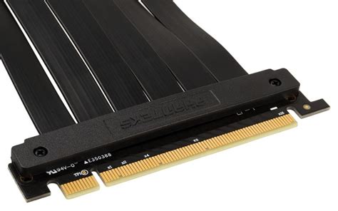 Read more: Top Factors that affect the flex printed circuit board price!
Material Selection One of the primary Factors Affecting Flex PCB Price is the choice of materials. The substrate, conductor, and coverlay materials used in the manufacturing process can greatly influence the overall cost. Substrate Materials The substrate is the foundation of the flex PCB, providing the necessary flexibility and stability. […]
-
 Read more: Discount PCB Fabrication – 20% Off for PCBs from RAY PCB
Why Choose RAY PCB for Your PCB Fabrication? RAY PCB is a trusted name in the PCB manufacturing industry, known for its commitment to quality, reliability, and customer satisfaction. Here are some reasons why you should consider RAY PCB for your next project: 1. State-of-the-Art Manufacturing Facilities RAY PCB boasts […]
-
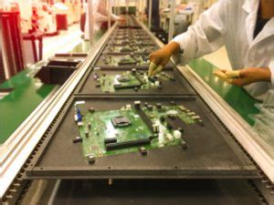 Read more: Top factors that can drive up PCB fabrication cost!
PCB Complexity and Design The complexity and design of a PCB are among the most significant factors influencing its fabrication cost. PCBs with intricate designs, high-density layouts, and multiple layers tend to be more expensive to manufacture than simpler, single-layer boards. Number of Layers The number of layers in a […]
-
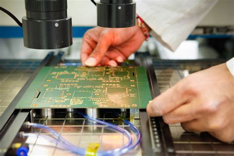 Read more: Demystifying PCB Fabrication: A Comprehensive Guide
What is PCB Fabrication? PCB fabrication is the process of creating printed circuit boards (PCBs) that are used to mechanically support and electrically connect electronic components. PCBs are essential in all but the simplest electronic devices. The fabrication process involves several steps to create the final board, including: Design and […]
-
Breakaway Tabs PCB: How to build and use one
Posted by
–
 Read more: Breakaway Tabs PCB: How to build and use one
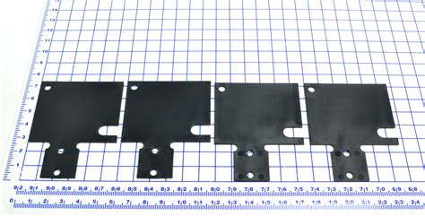
Introduction to Breakaway Tabs PCBs A breakaway tabs printed circuit board (PCB) is a convenient way to panelize and depanelize PCBs for manufacturing. The individual circuit boards are connected together into a larger panel by small tabs. After assembly, the individual boards can be easily snapped apart or “broken away” […]
-
Cost Analysis of PCB Assembly
Posted by
–
 Read more: Cost Analysis of PCB Assembly
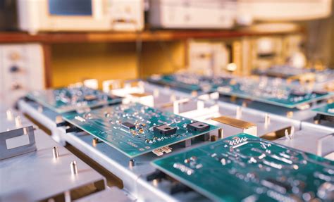
Introduction to PCB Assembly Costs Printed Circuit Board (PCB) assembly is a crucial process in the manufacturing of electronic devices. The cost of PCB assembly can significantly impact the overall production cost and profitability of a product. In this article, we will delve into the various factors that influence PCB […]


