Blog
-
 Read more: Manual Vs. Automated Assembly – Which one is right for you?
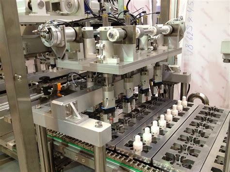
What is Manual Assembly? Manual assembly is a process where human workers use their hands, sometimes with the aid of simple tools, to put together components or sub-assemblies to create a final product. This method has been the traditional approach to assembly for centuries and is still widely used in […]
-
 Read more: How to Choose the Best Electronic Assembly Service?
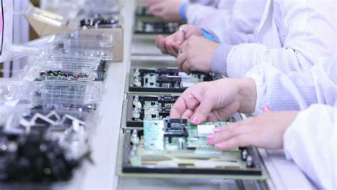
What is Electronic Assembly? Electronic assembly is the process of assembling electronic components onto a PCB to create a functional electronic device. This process involves several steps, including: PCB fabrication: The PCB is designed and manufactured according to the specific requirements of the electronic device. Component procurement: The necessary electronic […]
-
One-stop PCB Assembly Services
Posted by
–
 Read more: One-stop PCB Assembly Services
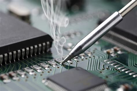
What is PCB Assembly? PCB Assembly, or Printed Circuit Board Assembly, is the process of attaching electronic components to a printed circuit board to create a functional electronic device or product. It involves soldering components onto the raw PCB, which is a non-conductive substrate made of fiberglass, copper traces, and […]
-
PCBA Manufacturing: A Step-by-Step Guide
Posted by
–
 Read more: PCBA Manufacturing: A Step-by-Step Guide
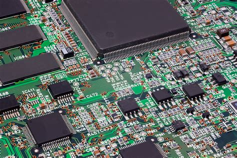
Introduction to PCBA Manufacturing PCBA (Printed Circuit Board Assembly) manufacturing is the process of assembling electronic components onto a printed circuit board (PCB) to create a functional electronic device. The process involves several steps, including PCB design, component sourcing, assembly, testing, and packaging. In this comprehensive guide, we will walk […]
-
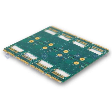 Read more: Reinvent Multilayer PCB Manufacturing with additive manufacturing!
Introduction to Multilayer PCB Additive Manufacturing Multilayer PCBs (Printed Circuit Boards) are essential components in modern electronics, enabling the creation of compact, high-performance devices. Traditional manufacturing methods for multilayer PCBs involve subtractive processes, such as etching and drilling, which can be time-consuming, wasteful, and limited in terms of design flexibility. […]
-
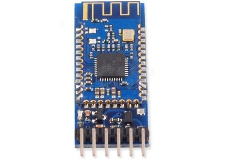 Read more: The best design guidelines for Bluetooth Circuit Boards!
Introduction to Bluetooth PCB Guidelines Bluetooth technology has become ubiquitous in modern electronic devices, enabling seamless wireless communication between devices. As a result, the demand for well-designed Bluetooth circuit boards has increased significantly. Designing a Bluetooth PCB requires careful consideration of various factors to ensure optimal performance, reliability, and cost-effectiveness. […]
-
The Classification of Soldered Thru-hole Pad
Posted by
–
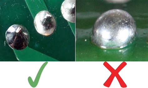 Read more: The Classification of Soldered Thru-hole Pad
Introduction to Solder-joint Classification Soldering is a critical process in the assembly of printed circuit boards (PCBs) and electronic components. The quality and reliability of solder joints directly impact the performance and longevity of electronic devices. In this article, we will focus on the classification of soldered through-hole pads, a […]
-
How much do you know about PCB Production?
Posted by
–
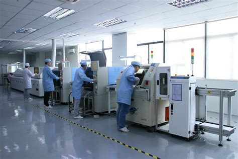 Read more: How much do you know about PCB Production?
What is PCB Production? PCB (Printed Circuit Board) production is the process of manufacturing electronic circuits by etching conductive pathways onto a non-conductive substrate. This process involves several steps, including designing the circuit layout, creating a photomask, applying photoresist, etching away unwanted copper, and finally, assembling components onto the board. […]
-
Drilling printed circuit boards
Posted by
–
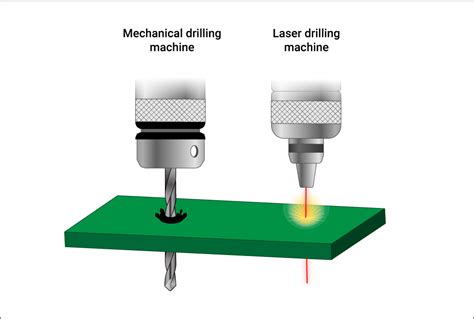 Read more: Drilling printed circuit boards
What is PCB Drilling? PCB drilling is the process of creating holes in a printed circuit board to accommodate electronic components, facilitate electrical connections between layers, and provide mounting points for the board itself. These holes are essential for the proper functioning and reliability of the PCB. Types of Holes […]
-
What is the typical tolerance for PCB?
Posted by
–
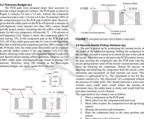 Read more: What is the typical tolerance for PCB?
What is PCB tolerance? PCB tolerance is the permissible deviation from the nominal or designed values for various aspects of a printed circuit board. These aspects include: Board dimensions Hole sizes and positions Conductor widths and spacing Solder mask and silkscreen alignment Component placement Tolerances are essential because manufacturing processes […]


