Blog
-
 Read more: Top benefits of Automation in Electronics Manufacturing!
Increased Productivity and Efficiency One of the most significant benefits of automation in electronics manufacturing is the boost in productivity and efficiency. Automated systems can work around the clock without breaks, fatigue, or human error, allowing manufacturers to increase their output and meet the growing demand for electronic devices. Faster […]
-
 Read more: Top Benefits of Contract Manufacturing PCB Assembly in USA!
Introduction to PCB Contract Manufacturing PCB (printed circuit board) contract manufacturing is the process of outsourcing the fabrication and assembly of PCBs to a specialized external company. Instead of investing in expensive equipment, facilities, and expertise to manufacture PCBs in-house, many electronics companies choose to partner with a contract manufacturer […]
-
 Read more: Top Causes of Warpage in PCB Assembly Process & Their Prevention Measures!
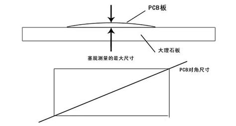
What is PCB Warpage? PCB warpage is a common issue in the PCB assembly process where the printed circuit board deforms or bends, resulting in an uneven surface. This can lead to various problems, such as poor component placement, reduced reliability, and increased manufacturing costs. Understanding the causes of PCB […]
-
 Read more: Top Challenges of Supply Chain Management in Electronics Manufacturing Industry! – How Your PCB Contract Manufacturer can Help?
The Importance of Supply Chain Management in Electronics Manufacturing Supply chain management is the process of overseeing the flow of goods and services from the point of origin to the point of consumption. In the electronics manufacturing industry, supply chain management is particularly important because of the complex nature of […]
-
Surviving Components Shortages Together
Posted by
–
 Read more: Surviving Components Shortages Together
The Root Causes of Components Shortages Several factors have contributed to the current components shortages: Increased Demand for Electronics The COVID-19 pandemic has accelerated the adoption of digital technologies, leading to a surge in demand for electronic devices. This sudden spike in demand has put pressure on manufacturers to ramp […]
-
IPC Releases Standard for Green Cleaners Used in Electronics Manufacturing for Public Review
Posted by
–
 Read more: IPC Releases Standard for Green Cleaners Used in Electronics Manufacturing for Public Review
New IPC-1402 Standard Defines Requirements for Environmentally Friendly Cleaning Agents The IPC (Association Connecting Electronics Industries) has released a new standard, IPC-1402, that establishes criteria for green cleaners used in electronics manufacturing. The “Standard for Green Cleaners Used in Electronics Manufacturing” aims to reduce the environmental impact of cleaning processes […]
-
Top Circuit Board Component Placement Guidelines
Posted by
–
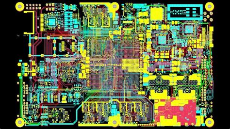 Read more: Top Circuit Board Component Placement Guidelines
Introduction to PCB Component Placement Proper placement of components on a printed circuit board (PCB) is critical for ensuring optimal performance, reliability, and manufacturability of the final product. PCB designers must consider various factors such as signal integrity, thermal management, electromagnetic compatibility (EMC), and assembly process constraints when determining the […]
-
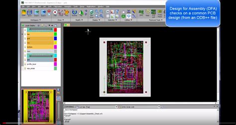 Read more: Top common mistakes to avoid while placing PCB assembly order!
Mistake 1: Failing to provide complete and accurate design files One of the most critical aspects of a successful PCB assembly order is providing the manufacturer with complete and accurate design files. This includes: Gerber files Bill of Materials (BOM) Pick and Place files Assembly drawings Gerber files Gerber files […]
-
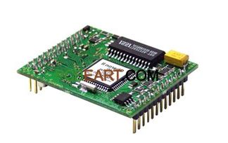 Read more: 6 Common PCB Assembly Mistakes and Their Corrective Actions
1. Incorrect Component Placement One of the most common mistakes in PCB assembly is incorrect component placement. This can happen due to human error, incorrect component labeling, or misinterpretation of the assembly drawing. Corrective Actions Double-check the assembly drawing and component labels before placing components Use automated component placement machines […]
-
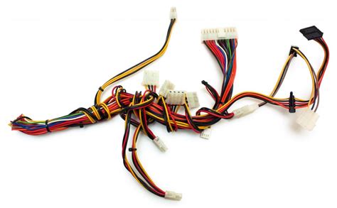 Read more: Top Considerations while selecting Cable and Wire Harness Assembly to enhance the performance of your final product!
Understanding Cable and Wire Harness Assembly Before diving into the considerations, let’s first understand what cable and wire harness assembly entails. A cable assembly is a group of cables or wires that are bundled together and terminated with connectors or other hardware. These assemblies are designed to transmit power, data, […]


