Blog
-
CABLE AND WIRE HARNESS ASSEMBLY
Posted by
–
 Read more: CABLE AND WIRE HARNESS ASSEMBLY
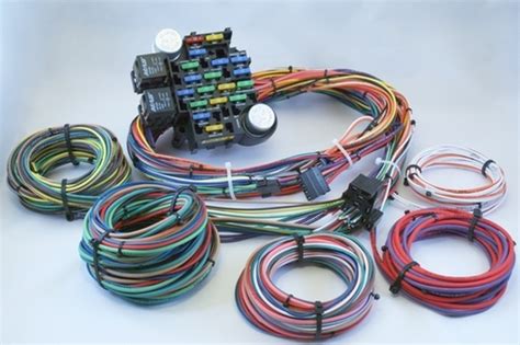
What is a Wire Harness? A wire harness, also known as a cable harness or wiring assembly, is a collection of wires, cables, and connectors that are bundled together to transmit signals or electrical power. Wire harnesses are used in various industries, including automotive, aerospace, telecommunications, and consumer electronics. They […]
-
 Read more: Find companies providing Electronic design services
What is Electronic design? Electronic design is the process of designing and developing electronic circuits, devices, and systems. It involves a wide range of activities, including: Circuit design and simulation PCB (Printed Circuit Board) layout and design Embedded software development FPGA (Field-Programmable Gate Array) design System integration and testing Electronic […]
-
 Read more: What Services Can You Expect from an Electronics Manufacturer?
Product Design and Development Concept Development and Feasibility Analysis The first step in creating a new electronic product is to develop a concept and assess its feasibility. An EMS provider can work with you to refine your idea, identify potential challenges, and determine the best approach for bringing your product […]
-
Several Noticing Points of PCB Silk Screen
Posted by
–
 Read more: Several Noticing Points of PCB Silk Screen
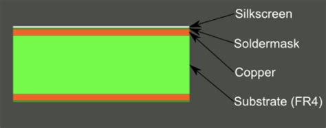
What is PCB Silkscreen? PCB silkscreen, also known as legend or nomenclature, is the text and symbols printed on the surface of a printed circuit board (PCB) to provide information about the board’s components, assembly instructions, and other important details. The silkscreen layer is typically applied using a screen printing […]
-
Electronic Manufacturing Services
Posted by
–
 Read more: Electronic Manufacturing Services
What is Electronic Manufacturing Services (EMS)? EMS providers offer a wide range of services, including: Design and engineering Prototype development Component sourcing and procurement PCB Assembly and testing Box build and system integration Logistics and distribution After-sales services and repairs By outsourcing these tasks to an EMS provider, OEMs can […]
-
 Read more: Why Is Electronic Contract Manufacturing Popular?
Cost Savings and Efficiency One of the primary drivers of Electronic Contract Manufacturing‘s popularity is the potential for significant cost savings and improved efficiency. By outsourcing production to a contract manufacturer, companies can: Avoid the high capital expenses associated with building and maintaining their own manufacturing facilities Leverage the contract […]
-
 Read more: What is Electronic Contract Manufacturing – Complete Guide
Introduction to Electronic Contract Manufacturing Electronic Contract Manufacturing (ECM) is a business model where a company, known as the contract manufacturer, produces electronic components or products for another company, known as the original equipment manufacturer (OEM). The OEM outsources the manufacturing process to the ECM provider, allowing them to focus […]
-
Challenges & top considerations to make your high-speed board design project successful!
Posted by
–
 Read more: Challenges & top considerations to make your high-speed board design project successful!
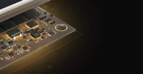
Introduction to High-Speed PCB Design High-speed PCB design is a complex process that requires careful consideration of various factors to ensure optimal performance and reliability. As technology advances and electronic devices become more sophisticated, the demand for high-speed PCBs continues to grow. However, designing high-speed PCBs comes with its own […]
-
 Read more: How to find the Perfect Electronic Assembly Company for your Industry?
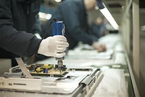
Introduction When it comes to manufacturing electronic products, finding the right Electronic Assembly company is crucial for the success of your project. Electronic assembly involves the process of assembling various electronic components onto a printed circuit board (PCB) to create a functional electronic device. Choosing the right partner can ensure […]
-
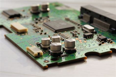 Read more: A Guide to PCBA: Definition, Types, Applications, and Process
What is PCBA? PCBA stands for Printed Circuit Board Assembly, which is the process of assembling various electronic components onto a printed circuit board (PCB) to create a functional electronic device. A PCB is a flat board made of insulating materials, such as fiberglass or plastic, with conductive pathways printed […]


