
Blog
-
Read more: Why Ball Grid Array (BGA) is important in PCB assembly?
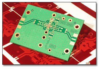
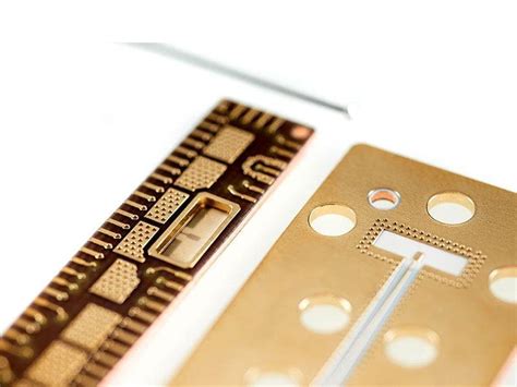
What is Ball Grid Array (BGA)? A Ball Grid Array (BGA) is a surface-mount package that utilizes a grid of solder balls on the bottom of the package to connect it to a PCB. The solder balls are arranged in a matrix pattern, allowing for a high density of connections […]
-
 Read more: Why Bill of Materials (BOM) is important in PCB Manufacturing process?
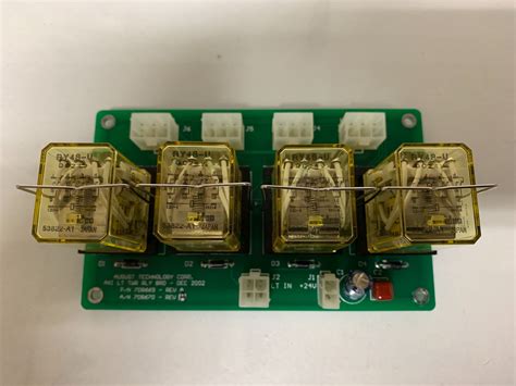
Introduction to BOM and its Significance in PCB Manufacturing In the world of electronics manufacturing, particularly in the realm of printed circuit boards (PCBs), the Bill of Materials (BOM) plays a crucial role. A BOM is a comprehensive list of all the components, materials, and quantities required to manufacture a […]
-
 Read more: Top Things about Fast PCB Prototyping that you must know!
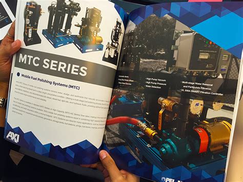
Introduction to PCB Prototyping PCB prototyping is an essential step in the development of electronic devices. It allows designers and engineers to test their designs and make necessary changes before mass production. Fast PCB prototyping is crucial for bringing products to market quickly and efficiently. In this article, we will […]
-
 Read more: Why choose Automated X-Ray Inspection (AXI) Technology in PCB Assembly?
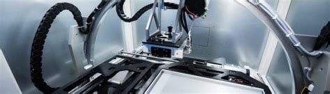
What is Automated X-Ray Inspection (AXI) Technology? Automated X-Ray Inspection (AXI) is a non-destructive testing method that utilizes X-rays to examine the internal structure and components of PCBs. Unlike traditional optical inspection techniques, AXI can penetrate through the layers of a PCB, providing a detailed view of solder joints, component […]
-
Automatic X-ray inspection (AXI)
Posted by
–
 Read more: Automatic X-ray inspection (AXI)
What is Automatic X-ray inspection (AXI)? Automatic X-ray Inspection (AXI) is a non-destructive testing method used to inspect the internal structure of manufactured products, particularly in the electronics industry. AXI systems utilize high-resolution X-ray imaging to detect defects, such as voids, cracks, and foreign objects, that may not be visible […]
-
 Read more: PCB Assembly Companies with Automated X-Ray Inspection (AXI)
Introduction to PCB AXI Automated X-Ray Inspection (AXI) is a crucial technology in the PCB assembly process that ensures the quality and reliability of printed circuit boards. AXI systems use advanced imaging techniques to detect defects and anomalies in PCBs that are not visible to the human eye. This non-destructive […]
-
 Read more: How to speed up your PCB prototypes from weeks to minutes!
Understanding the PCB prototyping Process Before we dive into the methods of accelerating PCB prototyping, let’s first understand the basic steps involved in the process: Design: Create the schematic and layout of the PCB using CAD software. Fabrication: Manufacture the physical PCB based on the design files. Assembly: Solder components […]
-
RAPID PCB PROTOTYPING
Posted by
–
 Read more: RAPID PCB PROTOTYPING
What is PCB Prototyping? PCB prototyping is the process of fabricating a small number of printed circuit boards, usually 1-100 pieces, to test and validate a design before committing to a larger production run. Prototypes allow engineers to: Verify the functionality and performance of the circuit design Test the physical […]
-
 Read more: Why is Metal Core Printed Circuit Board Widely Used in Led Products?
Introduction to Metal Core PCB Metal Core PCB, also known as MCPCB or thermal PCB, is a type of printed circuit board that utilizes a metal core as its base material instead of the traditional FR-4 substrate. The metal core, typically made of aluminum, provides excellent thermal conductivity, allowing for […]
-
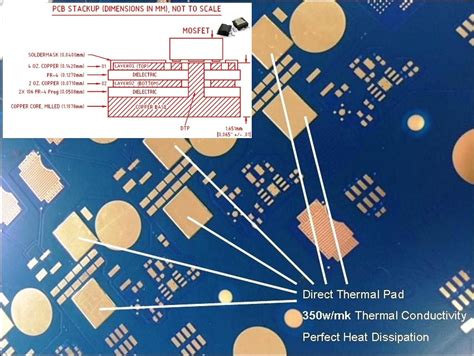
PCB Thermal Conductivity and Its Importance
Posted by
–
 Read more: PCB Thermal Conductivity and Its Importance
What is PCB Thermal Conductivity? PCB (Printed Circuit Board) thermal conductivity refers to the ability of a PCB material to conduct heat. It is a measure of how efficiently heat can transfer through the PCB, from the heat-generating components to the surrounding environment or heat sinks. Thermal conductivity is typically […]


