Blog
-
 Read more: Things to Consider While Choosing the Right PCB Manufacturer
Understanding Your PCB Requirements Before embarking on the search for a PCB Manufacturer, it is essential to have a clear understanding of your PCB requirements. This involves considering various aspects of your project, such as: PCB Complexity and Layer Count The complexity of your PCB design and the number of […]
-
Optimum PCB Design Flow
Posted by
–
 Read more: Optimum PCB Design Flow
Understanding the Importance of PCB Optimization PCB optimization is the process of refining and improving the design of a PCB to achieve the best possible performance while minimizing costs and potential issues. By optimizing the PCB design, engineers can: Enhance the overall functionality and reliability of the device Reduce manufacturing […]
-
Understanding Manufacturing Tolerances on a PCB – Track Width and Isolation Gap Tolerances
Posted by
–
 Read more: Understanding Manufacturing Tolerances on a PCB – Track Width and Isolation Gap Tolerances
What are PCB Tolerances? PCB tolerances refer to the acceptable variations in the dimensions and properties of a printed circuit board (PCB) during the manufacturing process. These tolerances are essential to ensure that the PCB functions as intended and meets the required specifications. Two critical aspects of PCB tolerances are […]
-
New CadSoft EAGLE DRU files for EAGLE V6
Posted by
–
 Read more: New CadSoft EAGLE DRU files for EAGLE V6
What are EAGLE DRU Files? EAGLE, which stands for Easily Applicable Graphical Layout Editor, is a powerful PCB design software used by engineers and hobbyists around the world. One of the key features of EAGLE is the ability to define design rules using Design Rule Check (DRC) files, also known […]
-
INDUSTRIAL PCB PROTOTYPE
Posted by
–
 Read more: INDUSTRIAL PCB PROTOTYPE
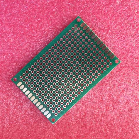
What is a PCB prototype? A PCB (printed circuit board) prototype is an early sample or model of a PCB used for testing and evaluations before mass production. PCB prototypes allow engineers to test the form, fit, and function of a new PCB design. They help verify the board layout, […]
-
PCB PROTOTYPE
Posted by
–
 Read more: PCB PROTOTYPE
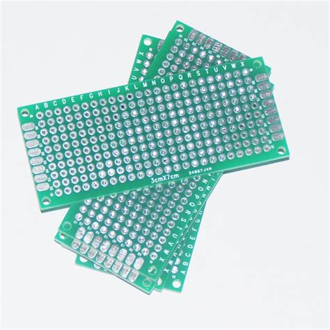
What is a PCB prototype? A PCB (Printed Circuit Board) prototype is a preliminary version of a printed circuit board that is used for testing and evaluation purposes before mass production. It is an essential step in the electronics manufacturing process, allowing designers and engineers to validate the functionality, performance, […]
-
 Read more: PCB Prototyping Paving Way For Innovations In The Marine Industry
The Role of PCBs in Marine Applications PCBs are essential components in a wide range of marine applications, from navigation and communication systems to propulsion and power management. These compact, lightweight, and reliable electronic circuits form the backbone of modern marine technology, enabling the integration of complex functions into small, […]
-
THROUGH HOLE PCB ASSEMBLY
Posted by
–
 Read more: THROUGH HOLE PCB ASSEMBLY
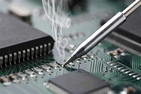
Introduction to PCB Assembly Printed Circuit Board (PCB) assembly is a crucial process in the manufacturing of electronic devices. It involves the mounting of electronic components onto a PCB to create a functional circuit. There are two main types of PCB assembly: through-hole and surface mount. In this article, we […]
-
What is a Multi-Layer PCB?
Posted by
–
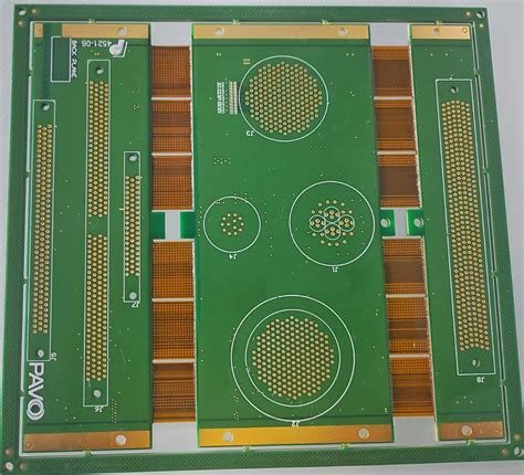 Read more: What is a Multi-Layer PCB?
Introduction to Multi-Layer Printed Circuit Boards A multi-layer printed circuit board (PCB) is a complex PCB that contains three or more conductive copper layers. These layers are laminated together with insulating material to form a single circuit board structure. Multi-Layer PCBs allow for much higher component density and more complex […]
-
What is a PCB Bare Board?
Posted by
–
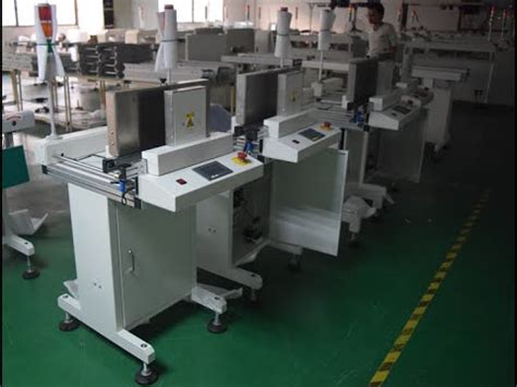 Read more: What is a PCB Bare Board?
Introduction to PCB Bare Boards A Printed Circuit Board (PCB) bare board, also known as a printed wiring board (PWB), is a base layer of insulating material that has conductive copper traces printed onto its surface. It serves as the foundation for assembling electronic components and creating functional circuits. PCB […]


