Introduction to PCB prototyping
PCB (Printed Circuit Board) prototyping is a crucial step in the development of new electronic products. It allows engineers and designers to test and refine their designs before committing to full-scale production. In this article, we will explore the process of PCB prototyping, its benefits, and how it can help you bring your new product to market quickly and efficiently.
What is PCB Prototyping?
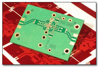
PCB prototyping is the process of creating a physical version of a PCB design for testing and validation purposes. This involves fabricating one or more copies of the PCB and assembling the necessary components onto it. The prototype can then be tested to ensure that it functions as intended and meets all the required specifications.
Benefits of PCB Prototyping
There are several key benefits to PCB prototyping:
-
Design Validation: Prototyping allows you to validate your PCB design and ensure that it functions as intended. This can help identify any issues or improvements that need to be made before moving to full-scale production.
-
Cost Savings: By identifying and addressing any issues during the prototyping phase, you can avoid costly mistakes and rework during production. This can result in significant cost savings in the long run.
-
Faster Time-to-Market: Prototyping allows you to quickly iterate on your design and make necessary changes. This can help accelerate the development process and bring your product to market faster.
-
Improved Quality: By thoroughly testing and refining your PCB design through prototyping, you can ensure a higher quality end product.
The PCB Prototyping Process
The PCB prototyping process typically involves the following steps:
1. Design Creation
The first step is to create the PCB design using specialized software such as Altium Designer, Eagle, or KiCad. This involves defining the circuit schematic, selecting components, and creating the physical layout of the board.
2. Design Review
Once the design is complete, it should be reviewed by experienced engineers to ensure that it meets all the necessary requirements and standards. This may involve running simulations, checking for potential issues, and making any necessary revisions.
3. Prototype Fabrication
After the design has been finalized, the prototype PCBs can be fabricated. This typically involves the following sub-steps:
-
PCB Fabrication: The PCB design files are sent to a PCB manufacturer, who will fabricate the bare boards according to the specified materials, layer count, and other requirements.
-
Component Sourcing: The necessary components for the prototype are sourced from suppliers. This may include both off-the-shelf components and custom parts.
-
PCB Assembly: The components are then assembled onto the fabricated PCB using methods such as through-hole assembly or surface-mount technology (SMT). This may be done manually for low-volume prototypes or using automated equipment for higher volumes.
4. Prototype Testing
Once the prototype PCBs have been assembled, they must be thoroughly tested to ensure that they function as intended. This may involve a range of tests, such as:
-
Functional Testing: Verifying that the PCB performs its intended functions correctly.
-
Signal Integrity Testing: Checking for any signal integrity issues, such as crosstalk or reflections.
-
Environmental Testing: Subjecting the PCB to various environmental conditions, such as temperature extremes or vibration, to ensure reliability.
-
Compliance Testing: Verifying that the PCB meets any necessary regulatory standards or certifications.
5. Design Iteration
Based on the results of the prototype testing, the PCB design may need to be revised and refined. This may involve making changes to the circuit design, component selection, or layout. The revised design can then be prototyped and tested again until the desired performance is achieved.

PCB Prototyping Technologies
There are several key technologies used in PCB prototyping:
PCB Fabrication Methods
-
Subtractive Methods: These involve starting with a copper-clad board and removing unwanted copper to create the circuit pattern. Common subtractive methods include etching and milling.
-
Additive Methods: These involve adding conductive material to create the circuit pattern. Examples include inkjet printing and 3D printing.
PCB Assembly Methods
-
Through-Hole Assembly: Components with wire leads are inserted through holes in the PCB and soldered in place. This method is well-suited for larger components and lower-volume production.
-
Surface-Mount Technology (SMT): Components are mounted directly onto the surface of the PCB. SMT allows for smaller components and higher-density designs, and is well-suited for automated assembly.
Rapid Prototyping Methods
-
3D Printing: Conductive and non-conductive materials can be 3D printed to create PCB Prototypes quickly. This method is well-suited for low-volume, complex designs.
-
Laser Prototyping: A laser can be used to selectively remove copper from a PCB to create the circuit pattern. This method is fast and well-suited for simple designs.

Choosing a PCB Prototyping Partner
When selecting a PCB prototyping partner, there are several key factors to consider:
-
Experience: Look for a partner with extensive experience in PCB prototyping and a track record of successful projects.
-
Capabilities: Ensure that the partner has the necessary equipment and expertise to handle your specific prototyping needs, such as multi-layer boards or high-density designs.
-
Quality: Choose a partner with strict quality control processes in place to ensure consistent, reliable results.
-
Turnaround Time: Consider the partner’s typical turnaround times and whether they can meet your project’s timeline.
-
Cost: Obtain quotes from multiple partners and compare pricing, but be cautious of sacrificing quality or reliability for lower costs.
| Factor | Considerations |
|---|---|
| Experience | – Extensive PCB prototyping experience – Track record of successful projects |
| Capabilities | – Equipment and expertise for specific needs – Ability to handle complex designs |
| Quality | – Strict quality control processes – Consistent, reliable results |
| Turnaround Time | – Typical turnaround times – Ability to meet project timeline |
| Cost | – Competitive pricing – Balance cost with quality and reliability |

FAQs
1. How long does PCB prototyping typically take?
The timeline for PCB prototyping can vary depending on the complexity of the design and the chosen prototyping methods. Simple designs using rapid prototyping methods may be completed in a few days, while more complex designs using traditional fabrication methods may take several weeks.
2. How much does PCB prototyping cost?
PCB prototyping costs can vary widely depending on factors such as the size and complexity of the design, the chosen fabrication and assembly methods, and the number of prototypes needed. Simple designs may cost a few hundred dollars, while complex, high-volume prototypes can cost several thousand dollars.
3. What are the most common PCB prototyping mistakes to avoid?
Some common mistakes to avoid in PCB prototyping include:
- Failing to properly review and validate the design before prototyping
- Not allowing sufficient time for prototyping and testing
- Choosing a prototyping partner based solely on cost, without considering quality and capabilities
- Not thoroughly testing the prototype under realistic conditions
- Rushing to production without fully refining the design based on prototype results
4. Can PCB Prototypes be used for final production?
In some cases, PCB prototypes may be suitable for low-volume production runs. However, prototypes are typically optimized for quick fabrication and testing, rather than for large-scale manufacturing efficiency. It’s generally best to use prototypes for design validation and refinement, and then optimize the design for full-scale production.
5. How can I ensure the best results from PCB prototyping?
To ensure the best results from PCB prototyping, follow these tips:
- Thoroughly review and validate your design before prototyping
- Choose an experienced, capable prototyping partner
- Allow sufficient time for prototyping and testing
- Test prototypes under realistic conditions
- Be prepared to iterate and refine the design based on prototype results
- Optimize the final design for manufacturability and scalability
Conclusion
PCB prototyping is a critical step in the development of new electronic products, allowing designers and engineers to validate and refine their designs before committing to full-scale production. By understanding the PCB prototyping process, technologies, and best practices, you can bring your new product to market quickly and efficiently while ensuring high quality and reliability.
When selecting a PCB prototyping partner, consider factors such as experience, capabilities, quality, turnaround time, and cost. By choosing the right partner and following best practices for design review, prototyping, and testing, you can achieve the best possible results and position your new product for success in the market.


Leave a Reply