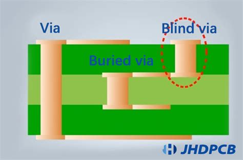
What are Blind Vias?
Blind vias are a type of interconnect used in printed circuit boards (PCBs) that start on an outer layer and terminate on an inner layer, without going through the entire thickness of the board. Unlike Through-Hole Vias, which penetrate all layers of the PCB, blind vias are “buried” within the board, making them invisible from the surface.
Advantages of Blind Vias
- Space-saving: By using blind vias, designers can save space on the outer layers of the PCB, allowing for more compact designs and increased component density.
- Improved signal integrity: Blind vias reduce the distance that signals need to travel, minimizing signal loss and improving overall signal integrity.
- Enhanced thermal management: Blind vias can be used to dissipate heat from high-power components, such as processors or power amplifiers, by providing a direct thermal path to inner layers of the PCB.
Manufacturing Process of Blind Vias
The manufacturing process for blind vias involves several steps:
- Drilling: Holes are drilled into the outer layers of the PCB using a laser or mechanical drill, stopping at the desired inner layer.
- Plating: The drilled holes are plated with a conductive material, typically copper, to create an electrical connection between the outer and inner layers.
- Filling: The plated holes are filled with a non-conductive material, such as epoxy resin, to provide structural support and prevent contamination.
- Lamination: The PCB Layers are laminated together under high pressure and temperature to create a solid, unified structure.
Comparison of Drilling Methods
| Method | Advantages | Disadvantages |
|---|---|---|
| Laser drilling | – High precision – Smaller hole sizes – Faster processing |
– Higher equipment costs – Limited material compatibility |
| Mechanical drilling | – Lower equipment costs – Wide material compatibility |
– Lower precision – Larger hole sizes – Slower processing |

Applications of Blind Vias
Blind vias are commonly used in various applications that require high-density interconnects, such as:
- Smartphones and tablets
- Wearable electronics
- Internet of Things (IoT) devices
- High-speed networking equipment
- Aerospace and defense systems
Example: Smartphone PCB with Blind Vias
In a modern smartphone, the PCB must accommodate a wide range of components, including the processor, memory, sensors, and RF modules, in a compact form factor. By using blind vias, designers can create a high-density interconnect structure that minimizes the PCB’s size while maintaining signal integrity and thermal performance.

Design Considerations for Blind Vias
When designing a PCB with blind vias, several factors must be considered:
- Via size and Aspect Ratio: The diameter and depth of the blind vias must be carefully chosen to ensure reliable plating and filling. The aspect ratio (depth to diameter) should be kept within manufacturable limits, typically less than 1:1.
- Layer stack-up: The placement of blind vias within the PCB layer stack-up must be optimized to minimize signal loss and crosstalk, while also considering the manufacturing feasibility and cost.
- Via pitch: The spacing between blind vias, known as via pitch, must be sufficient to prevent electrical and mechanical interference, while also allowing for reliable manufacturing.
- Material selection: The choice of PCB materials, such as the dielectric and conductor, must take into account the electrical, thermal, and mechanical requirements of the application, as well as the compatibility with the blind via manufacturing process.
Example: High-Speed PCB Layer Stack-up with Blind Vias
| Layer | Material | Thickness (mm) | Via Type |
|---|---|---|---|
| Top | Copper | 0.035 | Blind |
| Dielectric 1 | FR-4 | 0.2 | – |
| Inner 1 | Copper | 0.018 | Blind |
| Dielectric 2 | FR-4 | 0.4 | – |
| Inner 2 | Copper | 0.018 | – |
| Dielectric 3 | FR-4 | 0.4 | – |
| Bottom | Copper | 0.035 | – |
In this example, blind vias are used to connect the top layer to the first inner layer, while the second inner layer is connected using through-hole vias. The dielectric material and thickness are chosen to provide the desired electrical and mechanical properties, while the copper thickness is optimized for signal integrity and manufacturability.

Challenges and Limitations of Blind Vias
Despite their advantages, blind vias also present several challenges and limitations:
- Higher manufacturing costs: The additional drilling, plating, and filling steps required for blind vias increase the overall manufacturing cost compared to through-hole vias.
- Limited layer access: Blind vias can only connect outer layers to inner layers, but not inner layers to each other. For interconnects between inner layers, buried or through-hole vias must be used.
- Reduced thermal conductivity: The non-conductive fill material used in blind vias has lower thermal conductivity than the surrounding PCB material, which can limit the heat dissipation capability of the via.
- Potential reliability issues: If not designed and manufactured properly, blind vias can be susceptible to defects such as voids, cracks, or delamination, which can affect the reliability of the PCB.
Future Trends in Blind Via Technology
As electronic devices continue to become smaller, more powerful, and more complex, the demand for advanced interconnect technologies, such as blind vias, is expected to grow. Some of the future trends in blind via technology include:
- Smaller via sizes: Advances in laser drilling and plating technologies will enable the creation of even smaller blind vias, allowing for higher interconnect densities and more compact PCB designs.
- New materials: The development of new PCB materials, such as low-loss dielectrics and high-conductivity metals, will improve the electrical and thermal performance of blind vias.
- 3D packaging: Blind vias will play a crucial role in the development of 3D packaging technologies, such as package-on-package (PoP) and through-silicon via (TSV), which enable the vertical stacking of multiple chips or PCBs.
- Intelligent via placement: The use of advanced computer-aided design (CAD) tools and machine learning algorithms will optimize the placement and routing of blind vias, considering factors such as signal integrity, thermal management, and manufacturability.
Frequently Asked Questions (FAQ)
-
What is the difference between a blind via and a buried via?
A blind via connects an outer layer to an inner layer, while a buried via connects two or more inner layers without reaching the outer layers. -
Can blind vias be used in multilayer PCBs?
Yes, blind vias are commonly used in Multilayer PCBs to create high-density interconnects between outer and inner layers. -
What are the typical aspect ratios for blind vias?
The aspect ratio of a blind via (depth to diameter) is typically less than 1:1 to ensure reliable plating and filling. However, the exact ratio depends on the specific manufacturing process and PCB design requirements. -
How do blind vias affect the cost of PCB manufacturing?
Blind vias require additional drilling, plating, and filling steps compared to through-hole vias, which increases the overall manufacturing cost of the PCB. The cost impact depends on factors such as the number and size of the blind vias, the PCB material, and the manufacturing volume. -
Are there any limitations on the placement of blind vias in a PCB?
Yes, the placement of blind vias must consider factors such as the layer stack-up, via pitch, and signal integrity requirements. Designers must also ensure that the blind vias do not interfere with other components or features on the PCB, such as traces, pads, or planes.
In conclusion, blind vias are a crucial interconnect technology for creating high-density, high-performance PCBs in a wide range of applications. By understanding the manufacturing process, design considerations, and future trends of blind vias, engineers and designers can create more compact, reliable, and cost-effective electronic devices that meet the ever-increasing demands of the modern world.


Leave a Reply