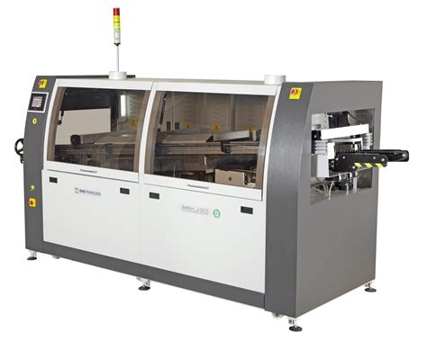
Introduction to Wave Soldering
Wave soldering is a widely used technique in electronic assembly manufacturing for soldering through-hole components to printed circuit boards (PCBs). It involves applying a wave of molten solder to the bottom side of a PCB, allowing the solder to flow through the holes and create electrical connections between the components and the board. Wave soldering has been a reliable method for decades, ensuring efficient and consistent results in high-volume production environments.
Benefits of Wave Soldering
- High throughput: Wave soldering enables the rapid soldering of multiple components simultaneously, making it suitable for high-volume production.
- Consistency: The automated nature of wave soldering ensures consistent solder joint quality across various boards, reducing the risk of human error.
- Cost-effectiveness: Wave soldering is a cost-effective solution for soldering through-hole components, especially in large-scale manufacturing.
- Versatility: Wave soldering can accommodate a wide range of component sizes and types, making it adaptable to different PCB designs.
Best Practices for Long-Term Success in Wave Soldering
To achieve long-term success in electronic assembly manufacturing using wave soldering, it is essential to follow best practices that ensure process stability, quality, and efficiency. Let’s explore some key areas to focus on:
1. PCB Design Considerations
Proper PCB design is crucial for successful wave soldering. Here are some guidelines to follow:
1.1 Component Placement
- Ensure adequate spacing between components to allow for proper solder flow and prevent bridging.
- Orient components in the same direction to facilitate solder flow and minimize shadowing effects.
- Avoid placing components too close to the edge of the board to prevent solder overflow.
1.2 Hole Size and Pad Design
- Use appropriate hole sizes for component leads to ensure a snug fit and prevent Solder wicking.
- Design pads with sufficient size and shape to accommodate solder fillets and provide mechanical strength.
- Consider using tear-drop pads for improved solder joint reliability.
1.3 Solder Mask and Silk Screen
- Apply solder mask to protect against solder bridging and improve solder joint definition.
- Use clear and accurate silk screen markings for component placement and orientation.
- Ensure proper alignment of solder mask openings with pads to prevent solder mask encroachment.
2. Solder Material Selection
Choosing the right solder material is essential for achieving reliable solder joints and meeting specific requirements. Consider the following factors:
2.1 Alloy Composition
- Select a solder alloy that is compatible with the components and PCB materials.
- Common alloys include tin-lead (SnPb) and lead-free alternatives like tin-silver-copper (SAC).
- Consider the melting point, wetting properties, and mechanical strength of the alloy.
2.2 Flux Type
- Choose a flux that is suitable for the solder alloy and the desired level of cleanliness.
- Fluxes can be categorized as no-clean, water-soluble, or rosin-based.
- Consider the activator strength, residue levels, and compatibility with cleaning processes.
3. Process Control and Optimization
Maintaining process control and continuously optimizing the wave soldering process is essential for consistent results. Key areas to focus on include:
3.1 Preheat and Cooling
- Ensure proper preheating of the PCB to activate the flux and prevent thermal shock.
- Control the preheat temperature and duration based on the PCB thickness and component requirements.
- Implement controlled cooling to minimize thermal stress and prevent component damage.
3.2 Solder Wave Parameters
- Optimize the solder wave height, velocity, and contact time to achieve proper solder penetration and filleting.
- Maintain the solder pot temperature within the recommended range for the selected alloy.
- Monitor and control the solder pot composition to maintain the desired alloy properties.
3.3 Flux Application
- Apply the appropriate amount of flux to ensure proper wetting and solder joint formation.
- Control the flux deposition rate and uniformity to prevent excessive or insufficient fluxing.
- Regularly maintain and clean the flux application system to prevent contamination.
4. Inspection and Quality Control
Implementing robust inspection and quality control measures is crucial for identifying and addressing any issues in the wave soldering process. Consider the following practices:
4.1 Visual Inspection
- Perform visual inspection of solder joints immediately after the wave soldering process.
- Look for defects such as bridging, insufficient solder, solder balls, or lifted components.
- Use magnification aids or automated optical inspection (AOI) systems for enhanced accuracy.
4.2 Automated Inspection
- Implement automated inspection techniques, such as 3D solder paste inspection (SPI) or X-ray inspection, for critical components or high-volume production.
- Automated inspection systems can detect defects that may be missed by visual inspection and provide data for process improvement.
4.3 Statistical Process Control (SPC)
- Collect and analyze process data, such as solder wave parameters and defect rates, to monitor process stability.
- Use SPC tools, such as control charts and process capability analysis, to identify trends and variations.
- Take corrective actions based on SPC data to maintain process control and improve quality.
5. Maintenance and Housekeeping
Regular maintenance and housekeeping practices are essential for ensuring the long-term reliability and efficiency of the wave soldering process. Consider the following:
5.1 Equipment Maintenance
- Perform scheduled maintenance on wave soldering equipment, including solder pot, conveyor system, and flux application system.
- Clean and inspect the solder nozzle, solder pot, and other critical components regularly.
- Calibrate and verify the accuracy of temperature and flow controls.
5.2 Solder Pot Management
- Monitor and maintain the solder pot composition to ensure consistent alloy properties.
- Regularly skim the solder pot surface to remove dross and impurities.
- Perform solder analysis to check for contamination or degradation of the alloy.
5.3 Cleanliness and Contamination Control
- Maintain a clean and organized work environment to prevent contamination of the PCBs and components.
- Implement proper handling and storage procedures for PCBs, components, and solder materials.
- Use appropriate cleaning methods, such as aqueous or solvent-based cleaning, to remove flux residues and contaminants.

FAQs
-
Q: What are the most common defects in wave soldering, and how can they be prevented?
A: Common defects in wave soldering include bridging, insufficient solder, solder balls, and lifted components. These defects can be prevented by optimizing the solder wave parameters, ensuring proper flux application, and implementing robust inspection and quality control measures. -
Q: How often should I perform maintenance on my wave soldering equipment?
A: The frequency of maintenance depends on the usage and conditions of your wave soldering equipment. It is recommended to follow the manufacturer’s guidelines and establish a regular maintenance schedule based on your production volume and requirements. Typically, daily, weekly, and monthly maintenance tasks should be performed to ensure optimal performance. -
Q: Can I use lead-free solder alloys in my wave soldering process?
A: Yes, lead-free solder alloys, such as tin-silver-copper (SAC), can be used in wave soldering. However, it is important to consider the compatibility of the alloy with your components and PCB materials, as well as the process adjustments required for lead-free soldering, such as higher soldering temperatures and different flux chemistries. -
Q: How can I optimize my wave soldering process for high-volume production?
A: To optimize your wave soldering process for high-volume production, consider the following practices: - Ensure proper PCB design and component placement for efficient solder flow and minimal defects.
- Implement automated inspection techniques, such as AOI and SPI, to detect defects quickly and accurately.
- Use statistical process control (SPC) to monitor process stability and identify improvement opportunities.
- Invest in high-quality wave soldering equipment with advanced features for process control and repeatability.
-
Continuously train and educate your operators on best practices and troubleshooting techniques.
-
Q: What are the key considerations for selecting a solder flux for wave soldering?
A: When selecting a solder flux for wave soldering, consider the following factors: - Compatibility with the solder alloy and PCB materials.
- Flux type (no-clean, water-soluble, or rosin-based) based on the desired level of cleanliness and residue.
- Activator strength and effectiveness in removing oxides and promoting solder wetting.
- Residue levels and compatibility with downstream cleaning processes, if applicable.
- Compliance with relevant industry standards and environmental regulations.

Conclusion
Wave soldering is a critical process in electronic assembly manufacturing, and implementing best practices is essential for achieving long-term success. By focusing on PCB design considerations, solder material selection, process control and optimization, inspection and quality control, and maintenance and housekeeping, manufacturers can ensure consistent and reliable solder joints while maximizing efficiency and productivity.
Continuous improvement and adaptation to new technologies and requirements are key to staying competitive in the ever-evolving electronics industry. By embracing best practices and investing in the right tools and training, manufacturers can leverage the full potential of wave soldering and deliver high-quality electronic assemblies to their customers.
| Aspect | Recommended Practices |
|---|---|
| PCB Design | – Ensure adequate component spacing – Use appropriate hole sizes and pad designs – Apply solder mask and accurate silk screen markings |
| Solder Material Selection | – Select compatible solder alloy and flux – Consider melting point, wetting properties, and mechanical strength – Choose flux based on desired cleanliness and residue levels |
| Process Control and Optimization | – Ensure proper preheating and cooling – Optimize solder wave parameters (height, velocity, contact time) – Control flux application and maintain system cleanliness |
| Inspection and Quality Control | – Perform visual inspection for defects – Implement automated inspection techniques (AOI, SPI, X-ray) – Use statistical process control (SPC) for process monitoring and improvement |
| Maintenance and Housekeeping | – Perform regular equipment maintenance – Monitor and maintain solder pot composition – Maintain cleanliness and control contamination |
By adhering to these best practices and continuously refining your wave soldering process, you can achieve long-term success in electronic assembly manufacturing, delivering high-quality products and satisfying customer requirements.


Leave a Reply