What is a Bed-of-Nails Test?
A bed-of-nails test, also known as a bed-of-pins test or a fixture test, is a method used in electrical testing to verify the functionality and quality of printed circuit boards (PCBs) and electronic assemblies. This test involves using a specialized fixture equipped with an array of spring-loaded pins, which make contact with specific test points on the device under test (DUT).
The bed-of-nails test fixture is designed to match the layout of the PCB or electronic assembly, with each pin corresponding to a specific test point. When the DUT is placed on the fixture, the pins make contact with the test points, allowing electrical signals to be applied and measured. This enables the testing system to detect short circuits, open circuits, and other manufacturing defects that may affect the performance of the product.
Advantages of Bed-of-Nails Testing
- High throughput: Bed-of-nails testing allows for rapid testing of multiple test points simultaneously, enabling efficient testing of large volumes of PCBs or electronic assemblies.
- Repeatability: The fixed nature of the test fixture ensures consistent and repeatable testing across multiple units, reducing the likelihood of human error.
- Adaptability: Bed-of-nails fixtures can be customized to accommodate various PCB designs and test requirements, making them suitable for a wide range of applications.
Limitations of Bed-of-Nails Testing
- High initial cost: Designing and manufacturing bed-of-nails fixtures can be expensive, particularly for complex PCB designs or low-volume production runs.
- Limited access: As PCB designs become more compact and components are placed closer together, it becomes increasingly difficult to access all the necessary test points using a bed-of-nails fixture.
- Potential for damage: The spring-loaded pins can potentially damage delicate components or solder joints if not properly designed or maintained.
How Does a Bed-of-Nails Test Work?
A bed-of-nails test system typically consists of the following components:
- Test fixture: The bed-of-nails fixture is a custom-designed board that holds the spring-loaded pins in the required configuration to match the test points on the DUT.
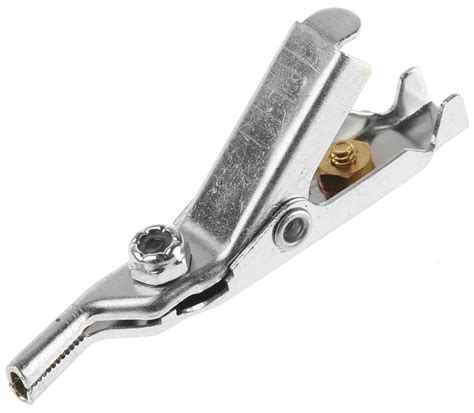
- Test pins: Spring-loaded pins, also called pogo pins, are used to make contact with the test points on the PCB or electronic assembly.
- Test electronics: The test system includes electronic instruments, such as digital multimeters, oscilloscopes, and function generators, to apply signals and measure responses from the DUT.
- Software: Test software is used to control the test instruments, execute test sequences, and analyze the results.
The testing process involves the following steps:
- Fixture preparation: The bed-of-nails fixture is set up with the appropriate test pins and connected to the test electronics.
- DUT placement: The PCB or electronic assembly is placed on the fixture, ensuring proper alignment with the test pins.
- Test execution: The test software initiates the test sequence, applying signals to the test points and measuring the responses.
- Result analysis: The measured responses are compared against the expected values to determine whether the DUT passes or fails the test.

Designing a Bed-of-Nails Fixture
Designing a bed-of-nails fixture involves several key considerations:
Test Point Selection
Identifying the appropriate test points on the PCB or electronic assembly is crucial for effective testing. Test points should be selected based on the following criteria:
- Accessibility: Test points should be easily accessible by the test pins without interfering with other components.
- Functionality: Test points should provide access to critical signals and nodes that are necessary for verifying the functionality of the DUT.
- Testability: Test points should enable the detection of common manufacturing defects, such as short circuits, open circuits, and component failures.
Pin Placement and Spacing
The placement and spacing of the test pins on the fixture must be carefully designed to ensure proper contact with the test points and to avoid interference with other components. Factors to consider include:
- Pin diameter: The diameter of the test pins should be selected based on the size of the test points and the required contact force.
- Pin spacing: The spacing between the pins should be sufficient to prevent short circuits and to accommodate any variations in the PCB layout.
- Component clearance: The test pins should be positioned to avoid contact with components on the PCB, particularly those with tall profiles or delicate structures.
Fixture Materials and Construction
The choice of materials and construction methods for the bed-of-nails fixture can impact its durability, reliability, and cost. Common materials used for fixtures include:
- FR-4: A glass-reinforced epoxy laminate, FR-4 is widely used for PCBs and offers good mechanical stability and electrical insulation properties.
- Acrylic: Clear acrylic sheets can be used for fixtures where visibility of the DUT is important, such as for visual inspection or debugging purposes.
- Aluminum: Machined aluminum fixtures offer high durability and dimensional stability, making them suitable for high-volume production testing.
The construction of the fixture should also consider factors such as:
- Alignment features: The fixture should include alignment features, such as guide pins or brackets, to ensure precise and repeatable positioning of the DUT.
- Connector interfaces: The fixture may require interfaces for connecting to the test electronics, such as edge connectors or cable assemblies.
- Maintenance access: The design should allow for easy access to the test pins and other components for maintenance and replacement purposes.

Test Strategies and Techniques
Effective bed-of-nails testing requires the development of appropriate test strategies and techniques to ensure comprehensive coverage of the DUT’s functionality. Some common test strategies include:
Continuity Testing
Continuity testing verifies that the electrical connections between test points are intact and free from open circuits. This can be achieved by applying a low-voltage signal to one test point and measuring the response at another test point. Continuity testing is particularly important for verifying the integrity of traces, vias, and solder joints.
Insulation Resistance Testing
Insulation resistance testing measures the resistance between isolated conductors, such as adjacent traces or pins, to ensure that there are no short circuits or leakage paths. This test typically involves applying a high-voltage DC signal between the conductors and measuring the resulting current flow. The measured resistance should exceed a specified minimum value to pass the test.
Functional Testing
Functional testing involves applying signals to the DUT’s inputs and measuring the responses at the outputs to verify that the device performs as intended. This may include tests such as:
- Logic testing: Verifying the functionality of digital circuits by applying test patterns and comparing the outputs to expected values.
- Analog testing: Measuring the performance of analog circuits, such as amplifiers, filters, and power supplies, by applying test signals and analyzing the output waveforms.
- Boundary scan testing: Utilizing built-in test features, such as JTAG or IEEE 1149.1, to test the interconnections and functionality of complex digital devices.
In-Circuit Testing
In-circuit testing involves measuring the performance of individual components on the PCB, such as resistors, capacitors, and integrated circuits, to ensure that they meet the specified tolerances. This test strategy requires the bed-of-nails fixture to provide access to the component terminals, allowing the test system to apply signals and measure the responses directly.

Test Automation and Data Management
As the complexity of PCBs and electronic assemblies increases, manual testing becomes increasingly time-consuming and error-prone. Test automation and data management tools can help streamline the bed-of-nails testing process and improve the efficiency and reliability of the results.
Test Automation Software
Test automation software, such as National Instruments TestStand or Keysight Technologies TestExec, provides a framework for developing and executing automated test sequences. These tools offer features such as:
- Test sequence development: Graphical interfaces and programming languages for creating and modifying test sequences.
- Instrument control: Drivers and APIs for communicating with test instruments and controlling their functions.
- Data logging and analysis: Tools for capturing, storing, and analyzing test results, including statistical analysis and trend monitoring.
- Reporting and documentation: Automated generation of test reports and documentation, including pass/fail status, measured values, and graphical results.
Data Management Systems
Data management systems, such as manufacturing execution systems (MES) or quality management systems (QMS), help organize and track test results throughout the manufacturing process. These systems offer benefits such as:
- Traceability: Associating test results with specific units, batches, or production runs, enabling traceability and root cause analysis.
- Statistical process control: Monitoring test results over time to identify trends, detect process variations, and initiate corrective actions.
- Integration with other systems: Exchanging data with other manufacturing systems, such as enterprise resource planning (ERP) or product lifecycle management (PLM), to provide a holistic view of the production process.
Best Practices for Bed-of-Nails Testing
To ensure the effectiveness and reliability of bed-of-nails testing, consider the following best practices:
- Collaborate with PCB designers: Involve the bed-of-nails test team early in the PCB design process to ensure that the board layout accommodates the required test points and facilitates efficient testing.
- Use standard test point designs: Adopt standard test point designs, such as vias or pads, to simplify the design of the bed-of-nails fixture and improve the reliability of the test connections.
- Implement design for testability: Incorporate testability features, such as boundary scan cells or built-in self-test (BIST) circuits, to enhance the controllability and observability of the DUT.
- Perform regular maintenance: Establish a maintenance schedule for the bed-of-nails fixture, including cleaning the test pins, replacing worn or damaged components, and verifying the alignment and contact force.
- Monitor and analyze test results: Regularly review test results to identify trends, detect anomalies, and initiate corrective actions to improve the quality and reliability of the products.
FAQ
1. What is the difference between a bed-of-nails test and a flying probe test?
A bed-of-nails test uses a fixed array of test pins to make contact with specific test points on the DUT, while a flying probe test uses movable probes that can be positioned to contact any point on the PCB. Bed-of-nails testing offers higher throughput and is suitable for high-volume production, while flying probe testing provides greater flexibility and is often used for prototyping or low-volume production.
2. Can bed-of-nails testing be used for both through-hole and surface-mount components?
Yes, bed-of-nails testing can be used for both through-hole and surface-mount components. However, the design of the test fixture and the selection of test points may differ depending on the component type and packaging.
3. How often should a bed-of-nails fixture be cleaned and maintained?
The frequency of cleaning and maintenance for a bed-of-nails fixture depends on factors such as the production volume, the type of components being tested, and the operating environment. As a general guideline, fixtures should be cleaned and inspected at least once per shift, with more frequent maintenance performed as needed based on the observed performance and wear of the test pins.
4. What is the typical cost of a bed-of-nails fixture?
The cost of a bed-of-nails fixture can vary widely depending on factors such as the complexity of the PCB design, the number of test points, and the materials and construction methods used. Simple fixtures for small PCBs may cost a few hundred dollars, while complex fixtures for large, high-density PCBs can cost several thousand dollars or more.
5. How can I ensure that my bed-of-nails test coverage is adequate?
To ensure adequate test coverage, consider the following strategies:
- Collaborate with PCB designers to identify critical test points and ensure that they are accessible by the bed-of-nails fixture.
- Use coverage analysis tools to assess the percentage of nodes, components, and functionalities that are tested by the bed-of-nails system.
- Perform regular audits of the test results to identify any gaps in coverage or areas where the test effectiveness may be compromised.
- Supplement bed-of-nails testing with other test methods, such as flying probe testing or functional testing, to provide additional coverage for areas that are difficult to access or test using the bed-of-nails fixture.
By implementing these strategies and continuously monitoring and improving the test process, you can ensure that your bed-of-nails testing provides comprehensive and reliable coverage of your PCBs and electronic assemblies.


Leave a Reply