Introduction to PCBs
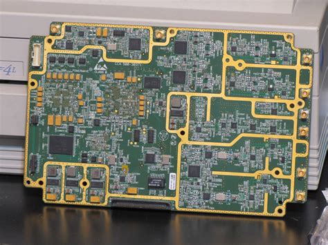
Printed Circuit Boards, commonly known as PCBs, are the backbone of modern electronic devices. These boards are used to mechanically support and electrically connect electronic components using conductive tracks, pads, and other features etched from copper sheets laminated onto a non-conductive substrate. PCBs have revolutionized the electronics industry by providing a reliable and efficient means of interconnecting electronic components in a compact and organized manner.
Types of PCBs
There are several types of PCBs, each designed to meet specific requirements and applications. The most common types include:
- Single-sided PCBs: These boards have conductive tracks on only one side of the substrate.
- Double-sided PCBs: These boards have conductive tracks on both sides of the substrate, allowing for more complex circuits and higher component density.
- Multi-layer PCBs: These boards consist of multiple layers of conductive tracks, separated by insulating layers, enabling even more complex circuits and higher component density.
- Flexible PCBs: These boards are made from flexible materials, allowing them to bend and conform to various shapes.
- Rigid-Flex PCBs: These boards combine the benefits of both rigid and flexible PCBs, with rigid sections for mounting components and flexible sections for connecting them.
PCB Manufacturing Process
The manufacturing process of PCBs involves several steps, each requiring precision and attention to detail. The main steps include:
- Design: The PCB layout is designed using specialized software, taking into account the required components, their placement, and the connections between them.
- Printing: The design is printed onto a photosensitive film, which is used to create a photomask.
- Etching: The photomask is used to expose the copper-clad board to UV light, hardening the areas that will form the conductive tracks. The unexposed areas are then etched away using a chemical solution.
- Drilling: Holes are drilled into the board to accommodate through-hole components and provide interconnections between layers.
- Plating: The holes are plated with a conductive material, typically copper, to ensure electrical continuity between layers.
- Solder Mask Application: A protective solder mask is applied to the board, covering the areas that should not be soldered.
- Silkscreen Printing: A silkscreen layer is printed onto the board, providing labels, logos, and other identifying information.
- Surface Finish Application: A surface finish, such as HASL (Hot Air Solder Leveling) or ENIG (Electroless Nickel Immersion Gold), is applied to protect the exposed copper and improve solderability.
- Electrical Testing: The completed board undergoes electrical testing to ensure that all connections are functioning as intended.
Advantages of Using Bare Board PCBs
Bare board PCBs, which are PCBs without any components mounted, offer several advantages over other interconnection methods:
Cost-effectiveness
One of the primary advantages of using bare board PCBs is their cost-effectiveness. By consolidating multiple electronic components onto a single board, manufacturers can reduce the overall cost of production. This is particularly true for high-volume production runs, where the cost per unit decreases significantly as the quantity increases.
Improved Reliability
Bare board PCBs offer improved reliability compared to other interconnection methods, such as point-to-point wiring or wire wrapping. By eliminating the need for individual wires and connectors, PCBs reduce the potential for connection failures and improve the overall reliability of the electronic device.
Increased Efficiency
The use of bare board PCBs streamlines the assembly process, increasing efficiency and reducing the time required to manufacture electronic devices. With components mounted directly onto the board, the need for manual wiring is eliminated, allowing for automated assembly processes that can produce devices more quickly and consistently.
Space Savings
Bare board PCBs enable manufacturers to create more compact electronic devices by allowing components to be mounted closer together. This is particularly important in applications where space is at a premium, such as in mobile devices, wearables, and aerospace electronics.
Enhanced Signal Integrity
PCBs are designed to maintain the integrity of electrical signals as they travel between components. By carefully controlling factors such as trace width, spacing, and impedance, designers can ensure that signals remain clear and free from interference, resulting in better overall device performance.

PCB Design Considerations
When designing a bare board PCB, several key factors must be considered to ensure optimal performance and reliability:
Component Placement
The placement of components on the PCB is crucial for several reasons. First, it affects the overall size and shape of the board, which can impact the final device’s form factor. Second, proper component placement can minimize the length of conductive tracks, reducing signal loss and interference. Finally, component placement must take into account factors such as heat dissipation and mechanical stress to ensure long-term reliability.
Signal Integrity
Maintaining signal integrity is essential for ensuring that the electronic device functions as intended. When designing a PCB, factors such as trace width, spacing, and impedance must be carefully controlled to minimize signal reflections, crosstalk, and other forms of interference. Additionally, proper grounding and shielding techniques must be employed to protect sensitive signals from external noise sources.
Power Distribution
Efficient power distribution is another critical consideration in PCB design. The power supply must be able to deliver the required current to all components without introducing noise or voltage drops. This requires careful planning of power planes, decoupling capacitors, and other power management techniques.
Thermal Management
As electronic components generate heat during operation, thermal management is an essential aspect of PCB design. Proper heat dissipation is necessary to prevent components from overheating, which can lead to reduced performance, reliability issues, and even device failure. Techniques such as the use of thermal vias, heat sinks, and proper component spacing can help to manage heat effectively.
Manufacturing Considerations
When designing a PCB, it is important to keep manufacturing considerations in mind. Factors such as minimum trace width, hole size, and spacing between components can impact the manufacturability of the board. By adhering to standard design guidelines and communicating with the manufacturer, designers can ensure that their boards can be produced efficiently and cost-effectively.

Common Applications of Bare Board PCBs
Bare board PCBs are used in a wide range of applications across various industries. Some of the most common applications include:
Consumer Electronics
Bare board PCBs are found in nearly all consumer electronic devices, including smartphones, tablets, laptops, televisions, and home appliances. In these applications, PCBs enable manufacturers to create compact, feature-rich devices that are reliable and cost-effective.
Industrial Electronics
In industrial settings, bare board PCBs are used in a variety of applications, such as process control systems, automation equipment, and data acquisition devices. These boards must be designed to withstand harsh environments, including exposure to extreme temperatures, vibration, and chemical contaminants.
Medical Devices
PCBs are essential components in many medical devices, including diagnostic equipment, patient monitoring systems, and implantable devices. In these applications, PCBs must meet stringent reliability and safety requirements to ensure patient safety and device effectiveness.
Automotive Electronics
The automotive industry relies heavily on electronic systems, and bare board PCBs are found in a wide range of automotive applications, including engine control units, infotainment systems, and advanced driver assistance systems (ADAS). Automotive PCBs must be designed to withstand the harsh environment of a vehicle, including exposure to extreme temperatures, vibration, and moisture.
Aerospace and Defense
In the aerospace and defense industries, bare board PCBs are used in a variety of applications, including avionics systems, communication equipment, and weapons systems. These boards must be designed to meet strict reliability and performance requirements, as well as withstand extreme environmental conditions.

Bare Board PCB Testing and Quality Control
To ensure the reliability and performance of bare board PCBs, manufacturers employ a range of testing and quality control measures:
Visual Inspection
The first step in PCB Quality Control is visual inspection. This involves examining the board for obvious defects, such as incorrect hole sizes, damaged traces, or contaminants on the surface of the board. Visual inspection can be performed manually or using automated optical inspection (AOI) equipment.
Electrical Testing
Electrical testing is performed to ensure that the PCB functions as intended and meets the specified electrical requirements. This can include continuity testing, which verifies that all connections are intact, and isolation testing, which ensures that there are no short circuits between adjacent traces. Other electrical tests may include impedance testing, voltage drop testing, and signal integrity testing.
Environmental Testing
Environmental testing is performed to ensure that the PCB can withstand the environmental conditions it will be exposed to during operation. This can include temperature cycling, humidity testing, vibration testing, and shock testing. These tests help to identify potential reliability issues and ensure that the board will perform as expected in its intended environment.
Functional Testing
Functional testing involves testing the PCB as part of a complete electronic system to ensure that it functions as intended. This can include testing the board’s ability to communicate with other components, verifying that it meets the specified performance requirements, and ensuring that it operates safely and reliably under normal and abnormal conditions.
Quality Management Systems
To ensure consistent quality and reliability, PCB manufacturers often implement quality management systems, such as ISO 9001 or AS9100. These systems provide a framework for continuous improvement and help to ensure that all processes, from design through manufacturing and testing, are performed consistently and effectively.
Future Trends in Bare Board PCB Technology
As electronic devices continue to evolve, so too will the technology behind bare board PCBs. Some of the key trends shaping the future of PCB technology include:
Miniaturization
The demand for smaller, more compact electronic devices is driving the trend toward miniaturization in PCB design. This involves the use of smaller components, finer trace widths and spacing, and more complex multi-layer board designs. As a result, PCB manufacturers are continually pushing the boundaries of what is possible in terms of board density and functionality.
High-Speed Design
As electronic devices become faster and more complex, PCB designers must contend with increasingly challenging signal integrity issues. High-speed design techniques, such as impedance matching, differential signaling, and careful control of trace geometry, are becoming increasingly important for maintaining signal quality and preventing interference.
Advanced Materials
The development of advanced PCB materials is another key trend in the industry. These materials, such as high-frequency laminates and low-loss dielectrics, are designed to improve signal integrity, thermal management, and mechanical performance. As electronic devices continue to push the boundaries of performance, the use of advanced materials will become increasingly important.
Embedded Components
Embedded components, such as capacitors, resistors, and even active devices, are becoming more common in PCB design. By embedding these components within the board itself, designers can save space, reduce the number of external components required, and improve overall system performance.
3D Printing
The use of 3D printing technology for PCB fabrication is an emerging trend that has the potential to revolutionize the industry. By using additive manufacturing techniques, it may be possible to create PCBs with complex geometries, embedded components, and other features that are difficult or impossible to achieve with traditional manufacturing methods.
Frequently Asked Questions (FAQ)
1. What is the difference between a bare board PCB and an assembled PCB?
A bare board PCB is a printed circuit board that does not have any electronic components mounted on it. An assembled PCB, on the other hand, is a board that has been populated with components and is ready for use in an electronic device.
2. What are the different types of bare board PCBs?
The main types of bare board PCBs include single-sided, double-sided, multi-layer, flexible, and rigid-flex boards. Each type has its own unique characteristics and is suited for different applications.
3. How are bare board PCBs manufactured?
The manufacturing process for bare board PCBs typically involves several steps, including design, printing, etching, drilling, plating, solder mask application, silkscreen printing, surface finish application, and electrical testing.
4. What are the advantages of using bare board PCBs?
Bare board PCBs offer several advantages, including cost-effectiveness, improved reliability, increased efficiency, space savings, and enhanced signal integrity.
5. What are some common applications of bare board PCBs?
Bare board PCBs are used in a wide range of applications, including consumer electronics, industrial electronics, medical devices, automotive electronics, and aerospace and defense systems.
Conclusion
Bare board PCBs are a crucial component in modern electronic devices, providing a reliable and efficient means of interconnecting electronic components. By understanding the different types of PCBs, their manufacturing process, and the key design considerations, engineers and manufacturers can create boards that meet the specific requirements of their applications.
As electronic devices continue to evolve, so too will the technology behind bare board PCBs. Trends such as miniaturization, high-speed design, advanced materials, embedded components, and 3D printing are shaping the future of the industry and driving innovation in PCB design and manufacturing.
By staying up-to-date with these trends and leveraging the latest technologies and techniques, manufacturers can create bare board PCBs that are more reliable, efficient, and cost-effective than ever before, enabling the development of new and innovative electronic devices across a wide range of industries.


Leave a Reply