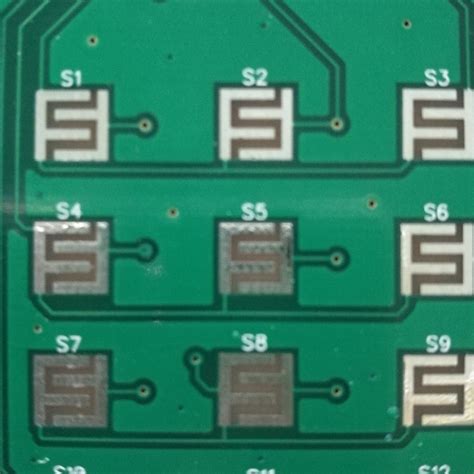
Introduction to PCB Carbon-Contacts
Printed Circuit Boards (PCBs) are essential components in modern electronics, providing a platform for interconnecting electronic components. One crucial aspect of PCB design and manufacturing is the application of contacts, which enable reliable electrical connections between the PCB and other components or devices. Among the various contact materials available, carbon contacts have gained significant attention due to their unique properties and advantages.
In this article, we will delve into the world of PCB carbon-contacts, exploring their characteristics, benefits, and the process of applying them to PCBs. We will also discuss the challenges associated with carbon contacts and provide insights into their applications in various industries.
What are Carbon Contacts?
Carbon contacts are electrical contacts made from carbon materials, such as graphite or carbon-based composites. These contacts are known for their excellent electrical conductivity, low contact resistance, and high durability. Carbon contacts are commonly used in switches, relays, and other electromechanical devices where reliable and long-lasting electrical connections are essential.
Properties of Carbon Contacts
Carbon contacts exhibit several unique properties that make them suitable for use in PCBs:
-
High Electrical Conductivity: Carbon contacts provide excellent electrical conductivity, allowing for efficient current flow and minimizing power losses.
-
Low Contact Resistance: The low contact resistance of carbon contacts ensures reliable electrical connections and reduces the risk of signal degradation or power dissipation.
-
Durability and Wear Resistance: Carbon contacts are highly durable and resistant to wear, making them ideal for applications that involve frequent switching or mechanical stress.
-
Chemical Stability: Carbon contacts are chemically inert and resistant to oxidation, corrosion, and other environmental factors that can degrade electrical performance over time.
-
Temperature Resistance: Carbon contacts can withstand high temperatures without significant degradation, making them suitable for use in harsh environmental conditions.

Benefits of Using Carbon Contacts in PCBs
Incorporating carbon contacts into PCBs offers several advantages:
-
Improved Reliability: The durability and wear resistance of carbon contacts ensure reliable electrical connections, reducing the risk of failures and improving the overall reliability of the PCB.
-
Enhanced Signal Integrity: The low contact resistance and high conductivity of carbon contacts minimize signal loss and distortion, resulting in improved signal integrity and performance.
-
Reduced Power Losses: The efficient current flow provided by carbon contacts helps reduce power losses, leading to improved energy efficiency and reduced heat generation.
-
Increased Lifespan: The resistance to wear and environmental factors contributes to the extended lifespan of carbon contacts, reducing the need for frequent replacements and maintenance.
-
Cost-Effectiveness: Carbon contacts offer a cost-effective solution compared to other contact materials, such as gold or silver, while still providing excellent performance characteristics.

Applying Carbon Contacts to PCBs
The process of applying carbon contacts to PCBs involves several steps to ensure proper adhesion, electrical conductivity, and overall reliability. Let’s explore the key steps involved in this process:
1. Surface Preparation
Before applying carbon contacts, the PCB surface must be thoroughly cleaned and prepared. This typically involves the following steps:
- Cleaning: The PCB surface is cleaned using solvents or aqueous solutions to remove any contaminants, such as dirt, grease, or oxidation.
- Roughening: The contact area on the PCB is roughened using abrasive methods, such as sandblasting or mechanical abrading, to create a suitable surface for adhesion.
- Activation: The PCB surface is chemically activated to enhance the adhesion of the carbon contact material.
2. Carbon Contact Material Selection
Choosing the appropriate carbon contact material is crucial for achieving the desired electrical and mechanical properties. Common carbon contact materials include:
- Graphite: Graphite is a widely used carbon contact material known for its excellent electrical conductivity and low contact resistance.
- Carbon-Polymer Composites: These composites combine carbon particles with polymer matrices to provide enhanced mechanical strength and wear resistance.
- Carbon Nanotubes: Carbon nanotubes offer exceptional electrical and thermal conductivity, making them promising candidates for high-performance carbon contacts.
The selection of the carbon contact material depends on factors such as the specific application requirements, environmental conditions, and cost considerations.
3. Carbon Contact Deposition
Once the PCB surface is prepared and the carbon contact material is selected, the next step is to deposit the carbon contacts onto the PCB. There are several methods for depositing carbon contacts:
- Screen Printing: Carbon contact paste is screen printed onto the PCB surface using a stencil or mesh screen. This method is suitable for large-scale production and allows for precise patterning of the carbon contacts.
- Ink-Jet Printing: Carbon contact ink is deposited onto the PCB using an ink-jet printer. This method offers high precision and flexibility in contact placement.
- Dispenser Deposition: Carbon contact paste is dispensed onto the PCB surface using a pneumatic or mechanical dispenser. This method is suitable for selective deposition and allows for precise control over the contact thickness.
The choice of deposition method depends on factors such as the desired contact geometry, production volume, and equipment availability.
4. Curing and Post-Processing
After the carbon contacts are deposited onto the PCB, they need to undergo a curing process to establish a strong bond with the PCB surface and achieve optimal electrical and mechanical properties. The curing process typically involves exposure to heat or ultraviolet (UV) light, depending on the specific carbon contact material and deposition method used.
Post-processing steps may include:
- Cleaning: Any residual material or debris is removed from the PCB surface to ensure clean and well-defined carbon contacts.
- Inspection: The PCB is visually inspected for any defects or irregularities in the carbon contacts, such as voids, cracks, or misalignment.
- Electrical Testing: The PCB undergoes electrical testing to verify the conductivity and resistance of the carbon contacts and ensure they meet the specified requirements.

Challenges and Considerations
While carbon contacts offer numerous benefits, there are also challenges and considerations to keep in mind when applying them to PCBs:
-
Adhesion: Ensuring proper adhesion between the carbon contacts and the PCB surface is critical for long-term reliability. Poor adhesion can lead to contact detachment or degradation over time.
-
Contact Resistance Variability: The contact resistance of carbon contacts can vary depending on factors such as the contact force, surface condition, and environmental factors. Careful design and process control are necessary to minimize variability.
-
Compatibility with Other Materials: Carbon contacts may not be compatible with certain PCB materials or finishes, such as gold or silver. Compatibility issues can lead to reduced performance or reliability.
-
Environmental Factors: Exposure to harsh environmental conditions, such as high temperatures, humidity, or chemical exposure, can affect the performance and lifespan of carbon contacts. Proper material selection and protective coatings may be necessary for demanding applications.
-
Cost Considerations: While carbon contacts are generally cost-effective compared to other contact materials, the overall cost of implementing carbon contacts in PCBs should be carefully evaluated, considering factors such as material costs, processing costs, and production volumes.
Applications of Carbon Contacts in PCBs
Carbon contacts find applications in various industries and sectors where reliable electrical connections and high-performance PCBs are essential. Some notable applications include:
-
Automotive Electronics: Carbon contacts are used in Automotive PCBs for applications such as engine control units, sensors, and power management systems, where durability and reliability are crucial.
-
Industrial Automation: PCBs with carbon contacts are employed in industrial automation systems, such as programmable logic controllers (PLCs), motor drives, and process control equipment, where robust and long-lasting electrical connections are required.
-
Consumer Electronics: Carbon contacts are used in PCBs for consumer electronic devices, such as smartphones, laptops, and wearables, to provide reliable and efficient electrical connections.
-
Medical Devices: PCBs with carbon contacts are utilized in medical devices, such as patient monitoring systems, diagnostic equipment, and implantable devices, where high reliability and long-term stability are critical.
-
Aerospace and Defense: Carbon contacts are employed in PCBs for aerospace and defense applications, such as avionics, communication systems, and military equipment, where performance and reliability under harsh environmental conditions are paramount.
Frequently Asked Questions (FAQ)
-
What are the advantages of using carbon contacts in PCBs compared to other contact materials?
Carbon contacts offer several advantages, including high electrical conductivity, low contact resistance, durability, wear resistance, chemical stability, and temperature resistance. They provide reliable electrical connections and improved signal integrity while being cost-effective compared to materials like gold or silver. -
How do I select the appropriate carbon contact material for my PCB application?
The selection of the carbon contact material depends on factors such as the specific application requirements, environmental conditions, and cost considerations. Common carbon contact materials include graphite, carbon-polymer composites, and carbon nanotubes. It is essential to evaluate the electrical and mechanical properties of each material and consult with PCB Manufacturers or material suppliers to make an informed decision. -
What surface preparation steps are necessary before applying carbon contacts to PCBs?
Before applying carbon contacts, the PCB surface must be cleaned to remove contaminants, roughened to create a suitable surface for adhesion, and chemically activated to enhance the bond between the carbon contact material and the PCB surface. These steps ensure proper adhesion and optimal electrical and mechanical performance of the carbon contacts. -
Can carbon contacts be used in high-temperature applications?
Yes, carbon contacts are suitable for high-temperature applications due to their temperature resistance. They can withstand elevated temperatures without significant degradation, making them ideal for use in harsh environmental conditions. However, it is essential to consider the specific temperature range and duration of exposure when selecting the appropriate carbon contact material and PCB design. -
Are there any challenges or considerations when applying carbon contacts to PCBs?
Yes, there are several challenges and considerations to keep in mind when applying carbon contacts to PCBs. These include ensuring proper adhesion between the carbon contacts and the PCB surface, managing contact resistance variability, considering compatibility with other PCB materials, and evaluating the impact of environmental factors on the performance and lifespan of the carbon contacts. Additionally, cost considerations should be carefully evaluated, taking into account material costs, processing costs, and production volumes.
Conclusion
Carbon contacts have emerged as a promising solution for achieving reliable and high-performance electrical connections in PCBs. With their excellent electrical conductivity, low contact resistance, durability, and resistance to wear and environmental factors, carbon contacts offer numerous benefits over traditional contact materials.
The process of applying carbon contacts to PCBs involves careful surface preparation, selection of the appropriate carbon contact material, deposition using methods such as screen printing or ink-jet printing, and post-processing steps to ensure optimal performance and reliability.
While there are challenges and considerations to keep in mind, such as adhesion, contact resistance variability, and compatibility with other materials, the advantages of carbon contacts make them a valuable option for a wide range of PCB Applications across various industries, including automotive, industrial automation, consumer electronics, medical devices, and aerospace and defense.
As technology continues to advance and the demand for high-performance PCBs grows, the use of carbon contacts is expected to gain further traction. Ongoing research and development efforts focus on improving the properties and processing techniques of carbon contact materials, opening up new possibilities for their application in PCBs.
By understanding the characteristics, benefits, and application process of carbon contacts, PCB designers, manufacturers, and end-users can leverage this technology to enhance the reliability, signal integrity, and overall performance of their electronic devices and systems.


Leave a Reply