The Importance of PCB Assembly in Electronics Manufacturing
PCB assembly plays a vital role in the production of electronic devices across various industries, including:
- Consumer electronics
- Automotive
- Aerospace
- Medical devices
- Industrial equipment
The quality and reliability of PCB assembly directly impact the performance and longevity of the final product. As such, understanding the industrial process of PCB assembly is essential for manufacturers, engineers, and product designers.
The PCB Assembly Process: An Overview
The PCB assembly process typically consists of the following main steps:
- PCB Design and Fabrication
- Solder Paste Application
- Component Placement
- Reflow Soldering
- Inspection and Testing
- Cleaning and Finishing
Let’s explore each of these steps in more detail.
PCB Design and Fabrication
Before the assembly process can begin, the PCB must be designed and fabricated. This involves the following sub-steps:
- Schematic Design: The electronic circuit is designed using specialized software, such as Altium Designer or KiCad.
- PCB layout: The physical layout of the PCB is created, including the placement of components, traces, and vias.
- Fabrication: The PCB is manufactured using a process called photolithography, which involves applying a photoresist layer, exposing it to UV light through a mask, and etching away the unwanted copper.
Solder Paste Application
Once the PCB is fabricated, the next step is to apply solder paste to the pads where components will be placed. This is typically done using one of two methods:
- Stencil Printing: A stencil with openings corresponding to the component pads is placed over the PCB, and solder paste is spread across the stencil using a squeegee. The stencil is then removed, leaving precise amounts of solder paste on the pads.
- Jet Printing: A specialized machine dispenses solder paste directly onto the pads using a jet printing process, which allows for greater flexibility and precision compared to stencil printing.
Component Placement
After the solder paste is applied, the components are placed onto the PCB. This is usually done using one of two methods:
- Pick and Place Machine: An automated machine picks up components from reels or trays and places them onto the PCB with high precision and speed. Modern pick and place machines can place thousands of components per hour.
- Manual Placement: For low-volume production or prototyping, components may be placed manually using tweezers or a vacuum pen.
Reflow Soldering
Once the components are placed, the PCB undergoes reflow soldering. This process involves heating the PCB in a controlled manner to melt the solder paste and form a permanent connection between the components and the PCB. The reflow soldering process typically consists of the following stages:
- Preheat: The PCB is gradually heated to activate the flux in the solder paste and prepare the components for soldering.
- Soak: The temperature is maintained to allow the components to reach thermal equilibrium and the flux to remove any oxides.
- Reflow: The temperature is raised above the melting point of the solder, causing the solder paste to melt and form a connection between the components and the PCB.
- Cooling: The PCB is cooled gradually to allow the solder joints to solidify and prevent thermal shock to the components.
Inspection and Testing
After reflow soldering, the PCB undergoes inspection and testing to ensure the quality and functionality of the assembly. This may include:
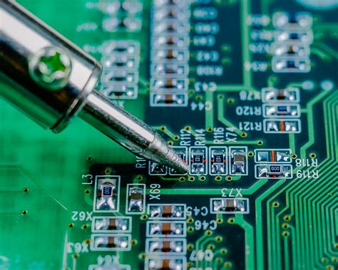
- Visual Inspection: The PCB is visually inspected for any defects, such as bridging, tombstoning, or misaligned components.
- Automated Optical Inspection (AOI): An automated system captures high-resolution images of the PCB and uses computer vision algorithms to detect any defects or anomalies.
- X-Ray Inspection: For complex assemblies with hidden solder joints, such as ball grid arrays (BGAs) or chip scale packages (CSPs), X-ray inspection may be used to verify the integrity of the solder connections.
- Functional Testing: The PCB is powered on and tested to ensure that it functions as intended, often using automated test equipment (ATE) or custom test fixtures.
Cleaning and Finishing
After inspection and testing, the PCB may undergo additional cleaning and finishing processes, such as:
- Flux Cleaning: Any remaining flux residue is removed from the PCB using a cleaning agent, such as isopropyl alcohol or a specialized flux cleaner.
- Conformal Coating: A protective coating is applied to the PCB to protect it from moisture, dust, and other environmental factors.
- Potting: For some applications, the PCB may be encased in a protective compound, such as epoxy or silicone, to provide additional mechanical and environmental protection.

PCB Assembly Techniques and Technologies
Several techniques and technologies are used in the PCB assembly process to ensure high-quality and efficient production. Some of these include:
Surface Mount Technology (SMT)
SMT is the most common PCB assembly technique, where components are mounted directly onto the surface of the PCB. SMT offers several advantages over through-hole technology, including:
- Smaller component sizes
- Higher component density
- Faster assembly speeds
- Lower production costs
Through-Hole Technology (THT)
THT involves inserting component leads through holes in the PCB and soldering them on the opposite side. While less common than SMT, THT is still used for certain components, such as connectors or large power devices, that require the mechanical strength provided by through-hole mounting.
Mixed Technology Assembly
Some PCBs may require a combination of SMT and THT components, known as mixed technology assembly. In this case, the SMT components are typically placed and soldered first, followed by the THT components.
Selective Soldering
For mixed technology assemblies or PCBs with components that are sensitive to high temperatures, selective soldering may be used. This process involves applying solder only to specific areas of the PCB using a localized heat source, such as a laser or a mini-wave soldering machine.
Automated Optical Inspection (AOI)
AOI systems use high-resolution cameras and computer vision algorithms to inspect PCBs for defects, such as component placement errors, solder bridge


Leave a Reply