China produces the majority of the world’s 99.6% alumina ceramic PCBs, and for good reason: mature supply chains for high-purity Al₂O₃ powder, established sintering and metallization infrastructure, and price points 30–50 % below comparable Western or Japanese sources. The trade-off is that factory quality varies widely, so qualifying a supplier takes real effort.
Why 99.6% Alumina Instead of 96%?
The jump from 96% to 99.6% purity eliminates most of the glassy silica binder phase. That change delivers measurably better electrical and thermal performance. Dielectric strength rises from roughly 10–15 kV/mm to 20–28 kV/mm (per ASTM D149). Thermal conductivity increases from 24–28 W/m·K to 30–35 W/m·K at 25 °C, depending on grain structure and density. Volume resistivity climbs above 10¹⁴ Ω·cm at room temperature.
These gains matter in power electronics, RF modules, high-voltage isolation substrates, and sensor packaging where 96% alumina’s lower resistivity or dielectric strength becomes a limiting factor. If your design does not push those limits, 96% alumina ceramic substrates cost less and are easier to machine—start there.
Key Properties of 99.6% Al₂O₃ Substrates
| Parameter | Value | Unit | Condition | Source |
|---|---|---|---|---|
| Al₂O₃ purity | ≥ 99.6 | % | — | CoorsTek ADS-996 |
| Density | 3.89–3.96 | g/cm³ | ASTM C373 | CoorsTek / Kyocera A-493 |
| Thermal conductivity | 30–35 | W/m·K | 25 °C, ASTM E1461 | CoorsTek ADS-996 |
| CTE | 7.9–8.4 | ppm/°C | 25–400 °C | Kyocera A-493 |
| Flexural strength | 350–400 | MPa | ASTM C1161, 4-pt bend | CoorsTek ADS-996 |
| Dielectric strength | 20–28 | kV/mm | ASTM D149, 1 mm thick | CoorsTek / Maruwa |
| Volume resistivity | > 10¹⁴ | Ω·cm | 25 °C | Kyocera A-493 |
| Surface roughness (as-fired) | 0.4–0.8 | µm Ra | — | Typical production |
| Surface roughness (polished) | ≤ 0.05 | µm Ra | — | Typical production |
Typical values for commercially available material, for comparison only. Confirm against the datasheet for your specific grade.
If your application demands surface roughness below 0.05 µm Ra for thin-film metallization or hermetic sealing, ask specifically about polished and lapped 99.6% alumina substrates.
What to Check When Qualifying a China Manufacturer
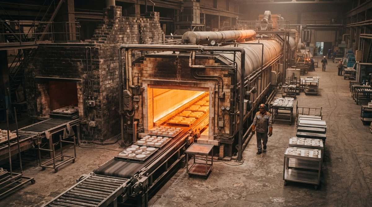
Not every factory advertising “99.6% alumina” actually sinters its own substrates. Many buy blanks from a handful of large Chinese powder-to-substrate producers (e.g., Liling or Xinxiang region kilns) and then perform only metallization and scribing. That is not inherently a problem, but you need to know which steps happen in-house so you can audit the right facility.
Factory Audit Checklist
- Powder sourcing and incoming QC. Ask for the Al₂O₃ powder COA (certificate of analysis). Purity, particle-size distribution (d50), and lot traceability should be documented.
- Sintering capability. High-purity alumina sinters at 1 600–1 750 °C in air or reducing atmosphere. Confirm kiln type (tunnel or batch), temperature uniformity (±5 °C or better), and whether sintering is in-house or outsourced.
- Metallization process. Thick-film (screen-printed Ag, Ag/Pd, Au), thin-film (sputtered Ti/Ni/Au, TiW/Au), or DPC (direct plated copper). Each has different line/space capability and adhesion strength. Get pull-test data per ASTM F1842.
- Dimensional inspection. Request Cpk data on substrate thickness and XY dimensions. A competent factory holds ±0.5 % on length/width and ±1 % on thickness for as-fired parts.
- Certifications. ISO 9001 is baseline. IATF 16949 matters for automotive. Ask for the certificate number and verify it on the registrar’s website—counterfeit ISO certificates exist.
Red Flags
- No COA for raw powder, or COA from an unverifiable source.
- Claiming “99.6%” but quoting thermal conductivity below 28 W/m·K—this often means the substrate is actually 99% or lower grade.
- Unwillingness to provide cross-section micrographs showing grain structure and metallization adhesion.
- Lead times shorter than 2 weeks for custom substrates with no stock program explanation.
Cost Drivers for 99.6% Alumina PCBs from China
Expect 99.6% substrates to cost 1.5–3× more than equivalent 96% parts, depending on size, metallization, and finish. The premium comes from higher-purity powder (roughly 2–4× the raw material cost), tighter sintering process control, and lower yield on fine-pitch metallization.
The biggest cost lever is quantity. A single prototype substrate may run $15–$40 each. At volumes above 1 000 pieces, unit cost drops 40–60 %. For volume pricing, explore wholesale 99.6% alumina ceramic PCBs.
Other factors that move the price: substrate thickness below 0.25 mm (higher breakage), polished surfaces, via holes, and multi-layer metallization. Gold finish (ENIG or electroplated Au) adds $0.03–$0.08 per cm² depending on gold thickness.
Typical Applications
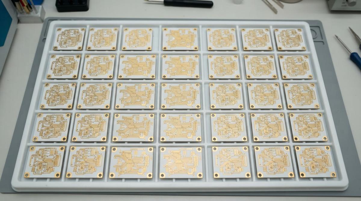
High-purity alumina sees heavy use in power semiconductor packaging (IGBT, SiC MOSFET baseplates), high-frequency RF and microwave circuits up to ~20 GHz, medical implant electronics requiring biocompatibility, and UV LED submounts where thermal and optical reflectivity both matter. For die-attach on ceramic substrates, 99.6% alumina provides a smoother, more consistent bonding surface than 96%.
When Not to Use 99.6% Alumina
If your thermal conductivity requirement exceeds 35 W/m·K, alumina—even at 99.6%—will not get you there. Move to aluminum nitride (AlN) substrates, which deliver 170–200 W/m·K at roughly 3–5× the cost of 99.6% alumina.
If your board needs plated through-holes, complex routing, or more than two metal layers, you are likely better served by LTCC or a hybrid approach. 99.6% alumina is a single- or double-sided substrate material, not a multilayer platform.
For cost-sensitive, moderate-performance designs—LED lighting, simple sensor boards, general industrial control—96% alumina does the job at lower cost and with more suppliers to choose from.
Import Considerations
Ceramic PCBs from China are classified under HTS codes that may carry tariffs depending on your country and the current trade policy environment. Factor in landed cost, not just FOB price. Confirm the HS code with your freight forwarder before committing to large orders.
FAQ
How do I verify a supplier’s alumina is actually 99.6% pure?
Request the raw powder certificate of analysis (COA) showing Al₂O₃ content ≥ 99.6% by mass, plus an XRF or ICP-OES report on the sintered substrate. Reputable factories provide these as standard documentation. If a supplier cannot produce them, look elsewhere.
Can I get custom shapes and laser scribing on 99.6% alumina?
Yes. CO₂ and Nd:YAG lasers both scribe 99.6% alumina cleanly. Snap lines, through-cuts, and complex profiles are standard offerings from most Chinese ceramic PCB factories. Tolerances of ±0.05 mm on laser-cut edges are achievable.
Is 99.6% alumina compatible with lead-free soldering?
It is. The substrate easily withstands SAC305 reflow profiles peaking at 245–260 °C. The limiting factor is metallization adhesion, not the ceramic itself. Confirm that the manufacturer’s thick-film or thin-film metal system is qualified for your specific solder alloy and reflow profile.
What is the typical MOQ from a Chinese 99.6% alumina manufacturer?
MOQs range from 1 piece (for prototypes at a premium) to 50–100 pieces for standard production runs. Factories prefer orders of 500+ pieces to justify setup costs. Below 50 pieces, expect per-unit pricing to be 2–3× the volume rate.
How does 99.6% alumina compare to AlN for RF applications?
At frequencies below ~20 GHz, 99.6% alumina (dielectric constant ~9.9, tan δ ~0.0001 at 1 MHz) performs well and costs far less than AlN. Above 20 GHz, AlN’s lower dielectric constant (~8.5) and higher thermal conductivity become meaningful advantages for power-dense RF designs.