Introduction to PCB Layers
Printed Circuit Boards (PCBs) are essential components in modern electronics. They provide a platform for mounting and interconnecting electronic components, enabling the creation of complex circuits. One crucial aspect of PCB design is the number and arrangement of layers within the board. In this article, we will delve into the world of PCB layers, exploring their types, functions, and the factors to consider when choosing the appropriate layer configuration for your project.
What are PCB Layers?
PCB layers are the individual sheets of conductive material, typically copper, that are laminated together to form a complete PCB. Each layer serves a specific purpose, such as carrying signals, providing power distribution, or offering shielding. The number of layers in a PCB can vary depending on the complexity and requirements of the circuit.
Why are PCB Layers Important?
The choice of PCB layers has a significant impact on several aspects of your project:
-
Circuit Complexity: More layers allow for greater routing flexibility and the ability to accommodate complex circuits with high component density.
-
Signal Integrity: Proper layer arrangement helps maintain signal integrity by minimizing crosstalk, reducing electromagnetic interference (EMI), and ensuring appropriate impedance control.
-
Power Distribution: Dedicated power and ground layers provide efficient and stable power distribution to components, reducing voltage drops and minimizing noise.
-
Board Size and Cost: The number of layers affects the overall thickness and cost of the PCB. More layers generally result in a thicker and more expensive board.
Types of PCB Layers
Let’s explore the different types of layers commonly found in PCBs:
1. Signal Layers
Signal layers are responsible for carrying the electrical signals between components on the PCB. They are typically located on the outer layers and inner layers of the board. The number of signal layers required depends on the complexity of the circuit and the routing requirements.
2. Power and Ground Layers
Power and ground layers, also known as plane layers, are dedicated to distributing power and providing a reference ground for the circuit. They ensure a stable and low-impedance power supply to the components. Having separate power and ground layers helps reduce noise and improve signal integrity.
3. Shielding Layers
Shielding layers, also called ground planes, are used to provide electromagnetic shielding between sensitive signal layers. They help reduce crosstalk and minimize the impact of external electromagnetic interference (EMI) on the circuit. Shielding layers are typically placed between signal layers or on the outer layers of the PCB.
4. Blind and Buried Vias
Blind and buried vias are specialized types of interconnects used in multi-layer PCBs. Blind vias connect an outer layer to an inner layer, while buried vias connect two or more inner layers without reaching the outer layers. These vias help optimize board space and improve signal routing in dense circuits.

Choosing the Right Number of PCB Layers
Determining the appropriate number of layers for your PCB project involves considering several factors:
1. Circuit Complexity
The complexity of your circuit is a primary factor in deciding the number of layers needed. More complex circuits with a higher component count and interconnections may require additional layers to accommodate efficient routing and minimize signal interference.
2. Signal Integrity Requirements
If your project demands high signal integrity, such as in high-speed digital circuits or sensitive analog designs, you may need to incorporate additional layers for proper shielding and impedance control. Dedicated power and ground layers, as well as shielding layers, can help maintain signal quality.
3. Board Size and Cost Constraints
The number of layers directly impacts the thickness and cost of the PCB. More layers result in a thicker board and higher manufacturing costs. Consider your project’s size and budget constraints when deciding on the layer count. Striking a balance between functionality and cost-effectiveness is crucial.
4. Manufacturing Capabilities
The capabilities of your chosen PCB manufacturer also play a role in determining the feasible number of layers. Some manufacturers may have limitations on the maximum number of layers they can produce or may require specific layer configurations. It’s essential to discuss your project requirements with the manufacturer to ensure compatibility.

Common PCB Layer Configurations
Here are some common PCB layer configurations and their typical applications:
| Layer Count | Configuration | Applications |
|---|---|---|
| 1 | Single-sided PCB | Simple circuits, low-cost projects |
| 2 | Double-sided PCB | General-purpose circuits, moderate complexity |
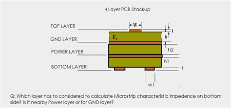
| 4 | Signal-Ground-Power-Signal | Moderate to complex circuits, improved noise immunity |
| 6 | Signal-Ground-Power-Power-Ground-Signal | Complex circuits, high-speed designs, better EMI Shielding |
| 8+ | Multiple signal, power, and shielding layers | High-density, high-speed, and sensitive analog circuits |

Best Practices for PCB Layer Design
To ensure optimal performance and manufacturability of your PCB, consider the following best practices:
-
Use dedicated power and ground layers: Incorporate dedicated power and ground layers to provide a low-impedance power distribution network and reduce noise.
-
Maintain proper layer symmetry: Ensure that the layer stackup is symmetrical to minimize warpage and improve manufacturing reliability.
-
Implement appropriate shielding: Use shielding layers strategically to reduce crosstalk and minimize EMI susceptibility.
-
Follow manufacturer’s design guidelines: Adhere to the design guidelines provided by your PCB manufacturer to ensure compatibility and optimal results.
-
Conduct thorough design reviews: Perform comprehensive design reviews to catch any potential issues related to layer configuration, signal integrity, and manufacturability.
FAQ
-
Q: How do I determine the number of layers needed for my PCB project?
A: The number of layers required depends on factors such as circuit complexity, signal integrity requirements, board size, and cost constraints. Evaluate your project’s specific needs and consult with your PCB manufacturer to determine the appropriate layer count. -
Q: Can I mix different types of layers in a single PCB?
A: Yes, it’s common to have a mix of signal, power, ground, and shielding layers in a single PCB. The specific arrangement and number of each layer type depend on the circuit requirements and design considerations. -
Q: What are the benefits of using dedicated power and ground layers?
A: Dedicated power and ground layers provide a low-impedance power distribution network, reducing voltage drops and minimizing noise. They help maintain a stable power supply to components and improve overall signal integrity. -
Q: How do blind and buried vias differ from regular vias?
A: Blind vias connect an outer layer to an inner layer, while buried vias connect two or more inner layers without reaching the outer layers. Regular vias, also known as through-hole vias, go through the entire thickness of the PCB, connecting all layers. -
Q: What are the cost implications of increasing the number of PCB layers?
A: Generally, adding more layers to a PCB increases the manufacturing cost. Each additional layer requires more materials, processing steps, and time. However, the cost increase is not always linear and depends on factors such as the PCB size, quantity, and manufacturer’s pricing structure.
Conclusion
Understanding PCB layers is crucial for designing reliable and high-performance electronic circuits. The number and arrangement of layers in a PCB have a significant impact on signal integrity, power distribution, and overall circuit functionality. By considering factors such as circuit complexity, signal requirements, board size, and cost, you can make informed decisions about the appropriate layer configuration for your project.
Remember to follow best practices, such as using dedicated power and ground layers, maintaining layer symmetry, and implementing proper shielding. Collaborating closely with your PCB manufacturer and conducting thorough design reviews will help ensure the success of your PCB project.
As you embark on your PCB design journey, keep in mind the importance of selecting the right number and type of layers to meet your project’s specific needs. With a solid understanding of PCB layers and careful consideration of design factors, you can create robust and reliable electronic devices that perform optimally.


Leave a Reply