What are PCB Pads?
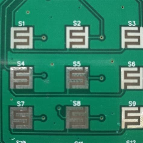
PCB pads, also known as solder pads or land patterns, are the exposed copper areas on a PCB where electronic components are soldered. They provide a conductive surface for the component leads or pins to make an electrical and mechanical connection with the board. Pads come in various shapes and sizes, depending on the component package and the specific design requirements.
Types of PCB Pads
There are several types of PCB pads, each designed to accommodate different component packages and mounting styles. Some common types include:
-
SMD (Surface Mount Device) Pads: These pads are used for surface-mounted components, such as resistors, capacitors, and integrated circuits (ICs). SMD pads are typically smaller than through-hole pads and have a flat surface for the component to sit on.
-
Through-Hole Pads: Through-hole pads are used for components with leads that pass through the PCB and are soldered on the opposite side. These pads have holes drilled in the center to allow the component leads to pass through.
-
BGA (Ball Grid Array) Pads: BGA pads are used for components with a grid of solder balls underneath, such as BGA packages for ICs. These pads consist of an array of circular pads that match the solder ball pattern on the component.
-
QFN (Quad Flat No-Lead) Pads: QFN pads are used for components with a flat, leadless package. They have a central thermal pad and peripheral pads for electrical connections.
-
Castellated Pads: Castellated pads are used for edge-mounted components or for connecting multiple PCBs together. They have half-circular pads along the edge of the board, allowing for easy soldering and mechanical stability.
Pad Sizes and Shapes
The size and shape of PCB pads are critical factors in ensuring proper component placement, solderability, and reliability. Pad dimensions are typically specified by the component manufacturer in their datasheet or application notes. Some key considerations for pad sizes and shapes include:
Pad Width and Length
Pad width and length are determined by the component lead or pin dimensions, as well as the soldering requirements. The pad should be large enough to provide sufficient area for a strong solder joint, but not so large that it causes unnecessary space consumption on the PCB.
For SMD components, the pad width is usually slightly larger than the component lead width to allow for proper soldering fillets. The pad length is determined by the component body size and the desired soldering area.
For through-hole components, the pad diameter should be larger than the lead diameter to allow for easy insertion and soldering. The pad length should be sufficient to accommodate the lead and provide enough space for soldering.
Pad Spacing
Pad spacing refers to the distance between adjacent pads on a PCB. Proper pad spacing is essential to prevent short circuits and ensure adequate insulation between conductors. The spacing requirements depend on factors such as the PCB manufacturing capabilities, the voltage and current levels, and the operating environment.
Industry standards, such as IPC (Association Connecting Electronics Industries), provide guidelines for minimum pad spacing based on the PCB design rules and the specific application requirements.
Pad Shape
The shape of PCB pads can vary depending on the component package and the design requirements. Some common pad shapes include:
- Rectangular pads: These are the most common shape for SMD components and provide a simple and efficient layout.
- Rounded rectangular pads: These pads have rounded corners to reduce stress concentrations and improve solder joint reliability.
- Circular pads: Circular pads are often used for through-hole components and can provide better centering and alignment during soldering.
- Oval pads: Oval pads are sometimes used for components with elongated leads or for providing additional soldering area.
The choice of pad shape depends on the specific component requirements, manufacturing capabilities, and design preferences.

Pad Design Considerations
Designing PCB pads requires careful consideration of various factors to ensure optimal performance, reliability, and manufacturability. Some key design considerations include:
Solder Mask Clearance
Solder mask is a protective coating applied to the PCB surface, leaving only the pads and other exposed areas for soldering. Solder mask clearance refers to the distance between the edge of the pad and the solder mask opening.
Proper solder mask clearance is important to prevent solder bridging and ensure a clean and reliable solder joint. The clearance should be sufficient to accommodate the solder fillets and prevent the solder mask from encroaching on the pad surface.
Industry standards, such as IPC-7351, provide guidelines for solder mask clearance based on the pad size and the PCB manufacturing capabilities.
Thermal Relief
Thermal relief is a design technique used to improve the solderability of pads connected to large copper areas, such as ground planes or power planes. It involves creating a pattern of narrow traces or spokes that connect the pad to the larger copper area.
Thermal relief helps to dissipate heat during soldering, preventing the pad from acting as a heat sink and making it easier to achieve a reliable solder joint. The thermal relief pattern should be designed to provide adequate electrical and thermal conductivity while allowing for efficient soldering.
Via Placement
Vias are conductive holes drilled through the PCB to connect different layers or to route signals between layers. When placing vias near pads, it is important to consider the spacing and the potential impact on the solder joint.
Vias should be placed at a sufficient distance from the pad to prevent solder wicking and ensure a reliable connection. The via size and the pad size should also be compatible to avoid manufacturing issues.
Industry standards provide guidelines for via placement and spacing to ensure proper manufacturability and reliability.
Pad Stacks
Pad stacks refer to the arrangement of pads on different layers of a multi-layer PCB. When designing pad stacks, it is important to consider the signal integrity, impedance control, and manufacturability.
Pad stacks should be designed to provide a continuous and consistent signal path through the PCB layers. The pad sizes and shapes should be consistent across layers to ensure proper alignment and avoid manufacturing issues.
For high-speed or impedance-controlled designs, the pad stack should be optimized to maintain the desired impedance and minimize signal reflections.

Best Practices for PCB Pad Design
To ensure optimal performance and reliability of PCB pads, consider the following best practices:
-
Follow component manufacturer recommendations: Always refer to the component datasheet or application notes for recommended pad sizes, shapes, and spacing.
-
Adhere to industry standards: Follow industry standards, such as IPC, for pad design guidelines and manufacturing tolerances.
-
Consider the manufacturing capabilities: Ensure that the pad design is compatible with the PCB manufacturing process and the specific fabrication capabilities.
-
Use appropriate solder mask clearance: Provide sufficient solder mask clearance around the pads to prevent solder bridging and ensure a clean solder joint.
-
Implement thermal relief for large copper areas: Use thermal relief patterns for pads connected to large copper areas to improve solderability and prevent heat sinking.
-
Optimize pad stacks for signal integrity: Design pad stacks to maintain consistent signal paths and control impedance in multi-layer PCBs.
-
Conduct design reviews and simulations: Perform thorough design reviews and simulations to verify the pad design, signal integrity, and manufacturability.
-
Test and validate the design: Conduct prototype testing and validation to ensure the pad design meets the performance and reliability requirements.

Frequently Asked Questions (FAQs)
-
What is the difference between SMD pads and through-hole pads?
SMD pads are used for surface-mounted components and have a flat surface for the component to sit on, while through-hole pads have holes drilled in the center to allow the component leads to pass through the PCB. -
How do I determine the appropriate pad size for a component?
The appropriate pad size for a component is usually specified in the component manufacturer’s datasheet or application notes. It depends on factors such as the component lead size, soldering requirements, and PCB manufacturing capabilities. -
What is solder mask clearance, and why is it important?
Solder mask clearance refers to the distance between the edge of the pad and the solder mask opening. It is important to provide sufficient clearance to prevent solder bridging and ensure a clean and reliable solder joint. -
What is thermal relief, and when should it be used?
Thermal relief is a design technique used to improve the solderability of pads connected to large copper areas. It involves creating a pattern of narrow traces or spokes that connect the pad to the larger copper area. Thermal relief should be used when a pad is connected to a ground plane, power plane, or any large copper area that can act as a heat sink during soldering. -
How can I ensure optimal signal integrity in pad stack design?
To ensure optimal signal integrity in pad stack design, consider the following: - Maintain consistent pad sizes and shapes across PCB layers.
- Optimize the pad stack geometry to control impedance and minimize signal reflections.
- Follow industry guidelines for pad stack design and manufacturing tolerances.
- Conduct simulations and tests to validate the signal integrity performance.
| Pad Type | Description | Application |
|---|---|---|
| SMD Pads | Used for surface-mounted components | Resistors, capacitors, ICs |
| Through-Hole Pads | Used for components with leads that pass through the PCB | Connectors, switches, large components |
| BGA Pads | Used for components with a grid of solder balls underneath | BGA packages for ICs |
| QFN Pads | Used for components with a flat, leadless package | QFN packages for ICs |
| Castellated Pads | Used for edge-mounted components or connecting multiple PCBs | Module interconnects, board-to-board connections |
In conclusion, PCB pads play a crucial role in the performance and reliability of electronic circuits. Understanding the types, sizes, shapes, and design considerations of pads is essential for creating robust and manufacturable PCB designs. By following industry standards, component manufacturer recommendations, and best practices, designers can ensure optimal pad design and achieve successful PCB assembly and operation.


Leave a Reply