Introduction to SMT Stencils and PCB prototyping
Printed circuit board (PCB) prototyping is an essential step in the development of electronic products. It allows engineers to test and validate their designs before moving to mass production. However, the process of PCB prototyping can be complex and time-consuming, especially when it comes to applying solder paste to the board for surface mount technology (SMT) components. This is where SMT stencils come in.
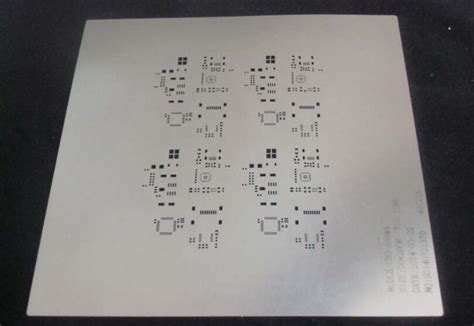
SMT stencils are thin metal sheets with openings that correspond to the pads on a PCB where solder paste needs to be applied. They are used in conjunction with a solder paste printer to precisely deposit the right amount of solder paste onto the PCB pads. This process is known as solder paste stencil printing.
The use of SMT stencils greatly simplifies the PCB prototyping process by ensuring accurate and consistent solder paste application. This article will explore how and why SMT stencils are utilized in PCB prototyping and the benefits they offer.
The Challenges of Applying Solder Paste in PCB Prototyping
Applying solder paste to a PCB is a critical step in the SMT assembly process. The solder paste serves as both an adhesive to hold the components in place and a conductive material to form electrical connections between the components and the PCB pads.
However, applying solder paste can be challenging, especially in PCB prototyping, where the quantities are small, and the designs may be complex. Some of the challenges include:
-
Accuracy: Applying the right amount of solder paste to each pad is crucial. Too little solder paste can result in poor connections, while too much can cause short circuits.
-
Consistency: Ensuring that the solder paste is applied consistently across all pads is essential for reliable performance.
-
Speed: Manually applying solder paste is a slow and tedious process, which can significantly increase the prototyping time.
-
Cost: Wasted solder paste due to inaccurate application can increase material costs.
These challenges can be overcome by using SMT stencils in the solder paste application process.

How SMT Stencils Work
An SMT stencil is a thin metal sheet, typically made of stainless steel or nickel, with openings that match the pads on a PCB. The stencil is placed on top of the PCB, and solder paste is applied using a squeegee or a solder paste printer.
As the squeegee or printer moves across the stencil, it forces the solder paste through the openings and onto the PCB pads. The stencil ensures that the right amount of solder paste is deposited on each pad and that the application is consistent across the entire board.
After the solder paste is applied, the stencil is lifted off the PCB, leaving precisely deposited solder paste on the pads, ready for component placement.

Benefits of Using SMT Stencils in PCB Prototyping
Using SMT stencils in PCB prototyping offers several benefits that simplify the process and improve the quality of the final product. Some of these benefits include:
-
Accurate solder paste application: SMT stencils ensure that the right amount of solder paste is deposited on each pad, reducing the risk of poor connections or short circuits.
-
Consistent results: Stencils provide a uniform solder paste application across the entire PCB, ensuring consistent performance of the assembled board.
-
Increased speed: Using SMT stencils with a solder paste printer automates the solder paste application process, significantly reducing the time required for prototyping.
-
Reduced material waste: Accurate solder paste application minimizes waste, reducing material costs.
-
Compatibility with various designs: SMT stencils can be customized to accommodate different PCB designs and pad sizes, making them suitable for a wide range of prototyping needs.
-
Improved quality: The precise solder paste application achieved with SMT stencils results in higher-quality solder joints, improving the overall reliability of the assembled PCB.

Choosing the Right SMT Stencil for PCB Prototyping
When selecting an SMT stencil for PCB prototyping, several factors should be considered to ensure optimal performance. These factors include:
Stencil Thickness
The thickness of the SMT stencil determines the amount of solder paste deposited on the PCB pads. The optimal stencil thickness depends on the size and pitch of the components being used. A general guideline for selecting stencil thickness based on component pitch is shown in the table below:
| Component Pitch | Recommended Stencil Thickness |
|---|---|
| > 0.65 mm | 0.100 – 0.125 mm |
| 0.5 – 0.65 mm | 0.100 – 0.115 mm |
| 0.4 – 0.5 mm | 0.075 – 0.100 mm |
| < 0.4 mm | 0.050 – 0.075 mm |
Aperture Size and Shape
The aperture size and shape of the SMT stencil should match the size and shape of the PCB pads. The aperture size is typically slightly smaller than the pad size to account for the solder paste’s tendency to spread during the reflow process.
Common aperture shapes include:
- Square
- Rectangular
- Circular
- Oblong
The choice of aperture shape depends on the specific design requirements and the type of components being used.
Stencil Material
SMT stencils are typically made of stainless steel or nickel. Stainless steel is the most common material due to its durability, ease of cleaning, and cost-effectiveness. Nickel stencils are less common but offer better wear resistance and are suitable for high-volume production.
Mounting Method
SMT stencils can be mounted on the solder paste printer using various methods, such as:
- Magnetic mounting
- Vacuum mounting
- Frame mounting
The choice of mounting method depends on the specific solder paste printer being used and the preferences of the operator.
The SMT Stencil Printing Process
The SMT stencil printing process involves several steps to ensure accurate and consistent solder paste application. These steps include:
-
Stencil alignment: The SMT stencil is aligned with the PCB using fiducial marks or alignment pins to ensure proper registration.
-
Solder paste application: Solder paste is applied to the stencil using a squeegee or a solder paste printer. The squeegee or printer moves across the stencil, forcing the solder paste through the apertures and onto the PCB pads.
-
Stencil removal: After the solder paste is applied, the stencil is carefully lifted off the PCB, leaving precisely deposited solder paste on the pads.
-
Inspection: The solder paste deposits are inspected visually or using automated optical inspection (AOI) equipment to ensure proper application and to detect any defects.
-
Component placement: After the solder paste is applied, the components are placed on the PCB using pick-and-place equipment or manual placement.
-
Reflow soldering: The PCB with the placed components is then subjected to a reflow soldering process, where the solder paste melts and forms permanent electrical and mechanical connections between the components and the PCB pads.
Maintaining and Cleaning SMT Stencils
To ensure consistent performance and a long lifespan, SMT stencils must be properly maintained and cleaned. Solder paste residue can build up on the stencil over time, affecting the quality of the solder paste deposits and potentially causing defects.
Regular cleaning of the SMT stencil is essential and can be done using various methods, such as:
- Manual cleaning with solvents and wiping materials
- Ultrasonic cleaning in a solvent bath
- Automated stencil cleaning systems
The choice of cleaning method depends on the type of solder paste being used, the frequency of cleaning required, and the available resources.
In addition to cleaning, SMT stencils should be inspected regularly for damage, such as bent or torn apertures, and replaced as necessary to maintain optimal performance.
Frequently Asked Questions (FAQ)
-
What is an SMT stencil?
An SMT stencil is a thin metal sheet with openings that correspond to the pads on a PCB where solder paste needs to be applied. It is used in conjunction with a solder paste printer to precisely deposit the right amount of solder paste onto the PCB pads. -
Why are SMT stencils used in PCB prototyping?
SMT stencils are used in PCB prototyping to simplify the process of applying solder paste to the board. They ensure accurate and consistent solder paste application, reduce material waste, and increase the speed of the prototyping process. -
How do I choose the right stencil thickness for my PCB Prototype?
The optimal stencil thickness depends on the size and pitch of the components being used. Refer to the table in the “Choosing the Right SMT Stencil for PCB Prototyping” section of this article for a general guideline on selecting stencil thickness based on component pitch. -
What materials are SMT stencils typically made of?
SMT stencils are typically made of stainless steel or nickel. Stainless steel is the most common material due to its durability, ease of cleaning, and cost-effectiveness. Nickel stencils offer better wear resistance and are suitable for high-volume production. -
How often should I clean my SMT stencil?
The frequency of cleaning depends on the type of solder paste being used and the volume of production. As a general rule, SMT stencils should be cleaned whenever a noticeable buildup of solder paste residue is observed or when print quality begins to deteriorate. Regular inspection and cleaning can help extend the lifespan of the stencil and maintain optimal performance.
Conclusion
SMT stencils play a crucial role in simplifying the PCB prototyping process by ensuring accurate and consistent solder paste application. By reducing material waste, increasing speed, and improving the quality of solder joints, SMT stencils help engineers and designers create better PCB Prototypes more efficiently.
When choosing an SMT stencil for PCB prototyping, it is essential to consider factors such as stencil thickness, aperture size and shape, stencil material, and mounting method to ensure optimal performance. Regular maintenance and cleaning of the stencil are also crucial for maintaining consistent results and extending the stencil’s lifespan.
As PCB designs continue to become more complex and compact, the use of SMT stencils in prototyping will remain an essential tool for electronics manufacturers looking to streamline their processes and deliver high-quality products to market quickly.


Leave a Reply