Introduction to Solder Paste printing
Solder paste printing is a crucial step in the Surface Mount Technology (SMT) assembly process. It involves depositing solder paste onto the printed circuit board (PCB) pads where components will be placed. Solder paste is a mixture of tiny solder particles suspended in flux, which helps to clean and protect the metal surfaces during the soldering process. Accurate and consistent solder paste printing is essential for achieving reliable and high-quality solder joints in SMT Assembly.
What is Solder Paste?
Solder paste is a thick, sticky mixture composed of the following ingredients:
- Solder alloy particles (typically tin, lead, and silver)
- Flux (rosin, activators, and solvents)
- Thickening agents
- Additives for improved printing and soldering performance
The solder alloy particles are usually spherical and range in size from 20 to 75 microns. The flux helps to remove oxides from the metal surfaces, prevents oxidation during the soldering process, and promotes wetting of the solder to the metal surfaces. Thickening agents, such as castor oil or hydrogenated castor oil, give the solder paste its desired viscosity and printability.
Solder Paste Classifications
Solder pastes are classified according to their particle size, flux type, and alloy composition. The most common classification system is the IPC J-STD-005, which defines solder paste types based on their particle size distribution and flux activity level.
| Type | Particle Size Range (microns) | Flux Activity Level |
|---|---|---|
| 1 | 20-38 | Low |
| 2 | 20-38 | Medium |
| 3 | 20-38 | High |
| 4 | 20-38 | Very High |
| 5 | 10-25 | Low |
| 6 | 10-25 | Medium |
| 7 | 10-25 | High |
| 8 | 10-25 | Very High |
Solder Paste Storage and Handling
Proper storage and handling of solder paste are critical for maintaining its quality and performance. Solder paste should be stored in a refrigerator at a temperature between 0°C and 10°C (32°F and 50°F) to prevent separation and degradation of the flux. Before use, the solder paste should be allowed to reach room temperature and thoroughly mixed to ensure consistent composition.
Solder Paste Printing Process
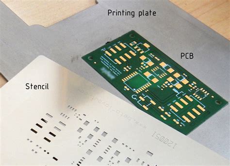
Stencil Design and Fabrication
The first step in solder paste printing is designing and fabricating a stencil. A stencil is a thin metal sheet (usually stainless steel) with apertures that correspond to the PCB pads. The aperture size and shape determine the amount and distribution of solder paste deposited on the pads.
Stencil thickness is another important factor, as it affects the volume of solder paste deposited. Typical stencil thicknesses range from 0.1 mm to 0.2 mm (4 to 8 mils), depending on the component size and pitch.
Stencils can be fabricated using various methods, such as:
- Laser cutting
- Chemical etching
- Electroforming
Printer Setup and Calibration
Before printing, the solder paste printer must be set up and calibrated to ensure accurate and consistent results. The following steps are typically involved:
- Aligning the stencil to the PCB using fiducial marks or vision systems
- Adjusting the squeegee pressure, speed, and angle
- Setting the print gap (distance between the stencil and PCB)
- Calibrating the solder paste dispenser
Modern solder paste printers often have automated features, such as vision systems for stencil-to-PCB alignment, closed-loop print pressure control, and automatic stencil cleaning.
Solder Paste Deposition
Once the printer is set up and calibrated, the solder paste is deposited onto the PCB pads through the following steps:
- The PCB is loaded onto the printer and aligned with the stencil.
- Solder paste is dispensed onto the stencil.
- A squeegee blade moves across the stencil, forcing the solder paste through the apertures and onto the PCB pads.
- The stencil is lifted, leaving the solder paste deposits on the PCB.
The print quality is influenced by several factors, including:
- Solder paste rheology (viscosity and thixotropy)
- Print speed and pressure
- Stencil design and condition
- PCB and pad surface finish
Solder Paste Inspection (SPI)
After printing, the solder paste deposits are inspected using a solder paste inspection (SPI) system. SPI systems use 2D or 3D imaging techniques to measure the volume, height, and shape of the solder paste deposits. This data is compared to predefined tolerances to identify any defects or inconsistencies, such as insufficient or excessive solder paste, bridging, or misalignment.
SPI systems can provide real-time feedback to the printer, allowing for automatic adjustments to maintain print quality. They also generate reports for process traceability and quality control.

Troubleshooting Common Solder Paste Printing Issues
Despite careful printer setup and calibration, solder paste printing issues can still occur. Some common issues and their potential causes include:
- Insufficient Solder paste
- Low print pressure
- Clogged stencil apertures
- Inadequate solder paste volume on the stencil
- Excessive solder paste
- High print pressure
- Oversized stencil apertures
- Excessive solder paste volume on the stencil
- Solder paste bridging
- Stencil apertures too close together
- Excessive solder paste volume
- Poor solder paste rheology
- Solder paste misalignment
- Poor stencil-to-PCB alignment
- PCB or stencil warpage
- Stencil stretch or deformation
To troubleshoot these issues, consider the following actions:
- Adjust print pressure, speed, or solder paste volume
- Clean or replace the stencil
- Modify stencil aperture size or shape
- Improve stencil-to-PCB alignment
- Optimize solder paste rheology
- Implement SPI for early defect detection and process control

Best Practices for High-Quality Solder Paste Printing
To achieve consistent, high-quality solder paste printing, follow these best practices:
- Use high-quality solder paste with appropriate rheology for your application
- Store and handle solder paste according to the manufacturer’s recommendations
- Design stencils with optimal aperture size, shape, and thickness
- Regularly clean and maintain the stencil and printer components
- Implement a robust printer setup and calibration procedure
- Monitor print quality using SPI and statistical process control (SPC) techniques
- Train operators on proper solder paste printing techniques and troubleshooting
- Establish and maintain a controlled environment (temperature, humidity, and cleanliness) for solder paste printing

Frequently Asked Questions (FAQ)
- What is the shelf life of solder paste?
-
The shelf life of solder paste depends on the specific product and storage conditions. Generally, solder paste can last up to 6 months when stored at the recommended temperature (0°C to 10°C or 32°F to 50°F) and up to 1 month at room temperature. Always consult the manufacturer’s data sheet for specific shelf life information.
-
How often should I clean my stencil?
-
Stencils should be cleaned regularly to prevent solder paste buildup and ensure consistent print quality. The cleaning frequency depends on factors such as the solder paste type, print volume, and environment. As a general rule, clean the stencil every 4-8 hours of continuous printing or whenever print quality issues arise.
-
What is the optimal print speed for solder paste printing?
-
The optimal print speed depends on the solder paste type, stencil design, and PCB layout. Typically, print speeds range from 20 to 200 mm/s. Slower speeds may be necessary for fine-pitch components or complex stencil designs, while higher speeds can be used for larger components or simpler layouts. Experiment with different speeds to find the best balance between print quality and throughput.
-
How do I choose the right solder paste for my application?
-
When selecting a solder paste, consider factors such as the alloy composition, particle size, flux type, and printing requirements. The alloy composition should match the melting temperature and mechanical properties required for your application. The particle size and flux type should be compatible with your stencil design and PCB Surface Finish. Consult with your solder paste supplier or manufacturer for recommendations based on your specific needs.
-
What is the difference between no-clean and water-soluble solder pastes?
- No-clean solder pastes have a flux that leaves a minimal, non-conductive residue after soldering, eliminating the need for post-soldering cleaning. Water-soluble solder pastes have a flux that requires cleaning with water or a mild solvent after soldering to remove the residue. No-clean solder pastes are more commonly used in SMT assembly due to their convenience and compatibility with most applications, while water-soluble solder pastes may be preferred for high-reliability or military applications where cleanliness is critical.
Conclusion
Solder paste printing is a critical step in SMT assembly that directly impacts the quality and reliability of solder joints. By understanding the properties of solder paste, implementing a robust printing process, and following best practices, manufacturers can achieve consistent, high-quality solder paste deposits. Regular monitoring, maintenance, and troubleshooting are essential for optimizing the solder paste printing process and ensuring the long-term success of SMT assembly operations.


Leave a Reply