Introduction to PCB Assembly Optimization
Printed Circuit Board (PCB) assembly is a crucial process in the manufacturing of electronic devices. Ensuring the correct component orientation during the assembly process is essential for the proper functioning and reliability of the final product. Optimizing the PCB assembly process not only improves the quality of the product but also reduces the chances of errors and rework, ultimately saving time and cost.
In this article, we will discuss the best practices for ensuring the correct component orientation during PCB assembly optimization. We will cover various aspects such as component placement, solder paste application, reflow soldering, and inspection techniques.
The Importance of Component Orientation in PCB Assembly
Correct component orientation is critical for several reasons:
- Functionality: Incorrectly oriented components may not function as intended, leading to circuit malfunctions or complete failure of the device.
- Reliability: Improperly oriented components can cause stress on the component leads or solder joints, leading to premature failure of the device.
- Manufacturability: Incorrect component orientation can cause issues during the assembly process, such as difficulty in placing the component or poor solder joint formation.

Best Practices for Ensuring Correct Component Orientation
1. Proper Component Placement
Proper component placement is the first step in ensuring correct component orientation. Here are some best practices to follow:
- Use a pick-and-place machine with vision systems to accurately place components on the PCB.
- Ensure that the component placement data is accurate and up-to-date.
- Use fiducial markers on the PCB to provide reference points for the pick-and-place machine.
- Use component polarity markers, such as a dot or a notch, to indicate the correct orientation of polarized components like diodes and electrolytic capacitors.
2. Solder Paste Application
Solder paste application is another critical step in the PCB assembly process. Here are some best practices to follow:
- Use a stencil with the correct aperture size and shape to apply solder paste to the PCB pads.
- Ensure that the stencil is properly aligned with the PCB to avoid misalignment of solder paste deposits.
- Use a solder paste inspection system to verify the correct volume and placement of solder paste on the PCB pads.
3. Reflow Soldering
Reflow soldering is the process of melting the solder paste to form a permanent electrical and mechanical connection between the components and the PCB. Here are some best practices to follow:
- Use a reflow oven with a well-defined temperature profile to ensure proper solder joint formation.
- Ensure that the PCB is properly supported during the reflow process to avoid warping or damage.
- Use a nitrogen atmosphere in the reflow oven to reduce oxidation and improve solder joint quality.
4. Inspection Techniques
Inspection is a critical step in ensuring the correct component orientation and overall quality of the PCB assembly. Here are some inspection techniques to consider:
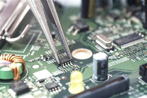
- Visual inspection: Trained operators can visually inspect the PCB assembly for correct component orientation and solder joint quality.
- Automated Optical Inspection (AOI): AOI systems use cameras and image processing algorithms to automatically inspect the PCB assembly for defects and incorrect component orientation.
- X-ray inspection: X-ray systems can be used to inspect solder joints and components that are hidden from view, such as Ball Grid Array (BGA) packages.
| Inspection Technique | Advantages | Disadvantages |
|---|---|---|
| Visual Inspection | – Low cost – Flexible – Can detect a wide range of defects |
– Subjective – Time-consuming – Limited to visible defects |
| Automated Optical Inspection (AOI) | – Fast – Objective – Can detect a wide range of defects |
– High initial cost – Limited to visible defects – May require programming |
| X-ray Inspection | – Can detect hidden defects – Objective – Non-destructive |
– High cost – Requires skilled operators – Limited to specific defect types |

Frequently Asked Questions (FAQ)
-
What is the most common cause of incorrect component orientation?
The most common cause of incorrect component orientation is human error during manual placement of components. This can be mitigated by using automated pick-and-place machines with vision systems. -
How can I ensure that polarized components are correctly oriented?
Polarized components, such as diodes and electrolytic capacitors, should have polarity markers, such as a dot or a notch, to indicate the correct orientation. These markers should be clearly visible on the component and the PCB Silkscreen. -
What is the purpose of fiducial markers on a PCB?
Fiducial markers are reference points on the PCB that are used by the pick-and-place machine to accurately place components. They help to compensate for any misalignment or distortion of the PCB during the manufacturing process. -
Can incorrect component orientation be detected by Automated Optical Inspection (AOI)?
Yes, AOI systems can detect incorrect component orientation by comparing the actual placement of the component with the expected placement based on the PCB design data. -
What are the consequences of incorrect component orientation?
Incorrect component orientation can lead to circuit malfunctions, complete failure of the device, and premature failure due to stress on the component leads or solder joints. It can also cause issues during the assembly process, such as difficulty in placing the component or poor solder joint formation.

Conclusion
Ensuring the correct component orientation is a critical aspect of PCB assembly optimization. By following best practices such as proper component placement, solder paste application, reflow soldering, and inspection techniques, manufacturers can improve the quality and reliability of their products while reducing the chances of errors and rework.
Investing in automated equipment, such as pick-and-place machines with vision systems and AOI systems, can significantly improve the accuracy and consistency of the PCB assembly process. However, it is also essential to have well-trained operators and a robust quality control system in place to catch any defects that may slip through the automated processes.
By prioritizing correct component orientation and implementing best practices throughout the PCB assembly process, manufacturers can deliver high-quality products to their customers while minimizing costs and maximizing efficiency.


Leave a Reply