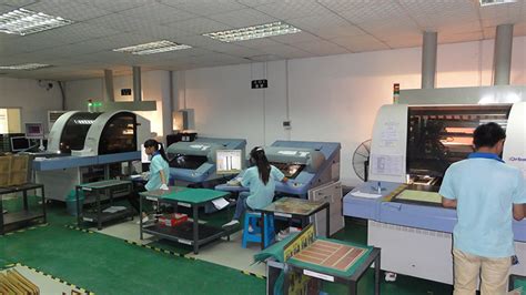
What is Automated Optical Inspection (AOI)?
Automated Optical Inspection (AOI) is a non-contact, image-based inspection technology used to verify the quality of PCBs during various stages of the assembly process. AOI systems employ high-resolution cameras, advanced lighting techniques, and sophisticated image processing algorithms to capture and analyze images of PCBs. These systems compare the captured images against a predefined set of design specifications or a “golden board” to identify any discrepancies or defects.
Benefits of AOI in PCB Assembly
- Early Defect Detection
- Increased Efficiency and Productivity
- Improved Product Quality and Reliability
- Cost Reduction
- Traceable Quality Control
Key Components of an AOI System
- Imaging System
- High-resolution cameras
- Lighting arrangements
- Lenses and filters
- Image Processing Software
- Defect detection algorithms
- Machine learning and artificial intelligence
- Statistical process control (SPC) tools
- Conveyor System
- PCB handling and transport
- Alignment and positioning mechanisms
- User Interface
- Operator controls and monitoring
- Defect classification and reporting

Types of AOI Systems
2D AOI Systems
2D AOI systems utilize top-down imaging to inspect the surface of PCBs. They are primarily used for detecting defects such as:
- Solder bridges
- Insufficient or excessive solder
- Component misalignment or absence
- Polarity issues
3D AOI Systems
3D AOI systems incorporate multiple cameras or structured light techniques to capture height information along with 2D images. This enables the detection of additional defects, including:
- Lifted or tilted components
- Coplanarity issues
- Solder volume and height variations
Inline vs. Offline AOI
- Inline AOI systems are integrated directly into the production line, inspecting PCBs immediately after the solder reflow process.
- Offline AOI systems are standalone units used for batch inspection or as a secondary inspection step.

Applications of AOI in PCB Assembly
- Solder Paste Inspection (SPI)
- Pre-Reflow Inspection
- Post-Reflow Inspection
- Final Assembly Inspection

Challenges and Limitations of AOI
- False Positives and False Negatives
- Component Variation and Complexity
- Reflective Surfaces and Shadowing
- High Initial Investment
Best Practices for Implementing AOI
- Establishing Inspection Criteria and Standards
- Optimizing Lighting and Image Acquisition
- Regular Calibration and Maintenance
- Operator Training and Skill Development
- Integration with Manufacturing Execution Systems (MES)
Leading AOI PCB Assembly Companies
| Company | Headquarters | Key Products/Services |
|---|---|---|
| Koh Young | South Korea | 3D SPI, 3D AOI, 3D MPI |
| Viscom | Germany | 3D AOI, X-ray Inspection |
| Omron | Japan | 3D AOI, SPI, AXI |
| Mirtec | South Korea | 3D AOI, SPI, AXI |
| Saki Corporation | Japan | 3D AOI, X-ray Inspection |
| Cyberoptics | USA | 3D SPI, 3D AOI, 3D MPI |
Future Trends in AOI PCB Assembly
- Artificial Intelligence and Deep Learning
- Improved defect detection and classification
- Adaptive algorithms for handling component variations
- Integration with Industry 4.0
- Real-time data collection and analysis
- Predictive maintenance and process optimization
- High-Resolution Imaging
- Advancements in camera technology
- Enhanced defect detection for miniaturized components
- Inline 3D CT Inspection
- Combining 3D AOI with computed tomography
- Non-destructive internal inspection of complex assemblies
Frequently Asked Questions (FAQ)
1. What is the difference between AOI and visual inspection?
AOI is an automated process that uses machine vision technology to inspect PCBs, while visual inspection relies on human operators to manually check for defects. AOI offers higher speed, consistency, and accuracy compared to manual inspection.
2. Can AOI completely replace human inspection?
While AOI significantly reduces the need for human inspection, it is not a complete replacement. Human operators are still required for programming, monitoring, and reviewing AOI results. Additionally, some complex defects may require manual verification.
3. How does AOI handle different component types and sizes?
Modern AOI systems are equipped with advanced algorithms and machine learning capabilities that allow them to adapt to different component types and sizes. The inspection criteria can be customized based on the specific requirements of each PCB design.
4. What is the typical defect detection rate of AOI systems?
The defect detection rate of AOI systems varies depending on factors such as PCB complexity, component density, and the specific AOI technology used. However, high-end AOI systems can typically achieve defect detection rates exceeding 90%.
5. How does AOI fit into the overall quality control process?
AOI is an integral part of the quality control process in PCB assembly. It complements other inspection techniques such as X-ray inspection, in-circuit testing, and functional testing. AOI helps identify defects early in the assembly process, reducing rework costs and improving overall product quality.
Conclusion
Automated Optical Inspection (AOI) has revolutionized the PCB assembly process by providing a fast, accurate, and reliable means of detecting defects and ensuring product quality. As electronic devices continue to become more complex and miniaturized, the role of AOI in PCB assembly will only grow in importance. AOI PCB assembly companies are at the forefront of this technological advancement, offering cutting-edge solutions that combine machine vision, artificial intelligence, and data analytics.
By embracing AOI technology, manufacturers can improve their production efficiency, reduce costs, and deliver high-quality products to their customers. As the industry evolves, we can expect to see further innovations in AOI, such as the integration of deep learning algorithms, inline 3D CT inspection, and seamless integration with Industry 4.0 frameworks.
In conclusion, AOI PCB assembly is a critical aspect of modern electronics manufacturing, and its significance will only continue to grow in the years to come. By partnering with leading AOI PCB assembly companies and adopting best practices in implementation, manufacturers can stay ahead of the curve and deliver products that meet the highest standards of quality and reliability.


Leave a Reply