Introduction to Blind Vias
In the world of printed circuit board (PCB) design, vias play a crucial role in interconnecting different layers of a multi-layer PCB. Among the various types of vias, blind vias have gained significant importance due to their ability to optimize board space and improve signal integrity. This article will delve into the concept of blind vias, their manufacturing process, advantages, and applications.
What are Vias?
Before exploring blind vias, let’s first understand what vias are. Vias are small holes drilled through a PCB to establish electrical connections between different layers of the board. They are essential for routing signals and power between components on different layers, enabling more complex and compact PCB designs.
Types of Vias
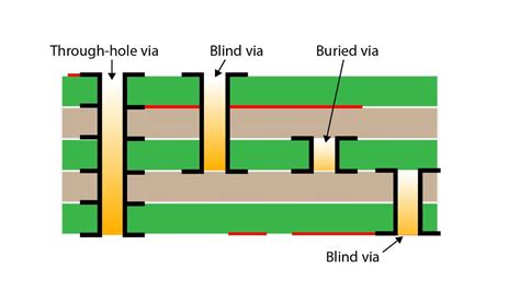
There are three main types of vias used in PCB design:
- Through Vias: These vias extend through all layers of the PCB, from the top to the bottom layer.
- Blind Vias: Blind vias are visible only on one side of the PCB and connect an outer layer to one or more inner layers, but do not extend through the entire board.
- Buried Vias: Buried vias are hidden within the inner layers of the PCB and do not reach either the top or bottom layer.
What is a Blind Via?
A blind via, also known as a partial via or hidden via, is a type of via that connects an outer layer of a PCB to one or more inner layers, but does not extend through the entire board. Unlike through vias, which are visible on both sides of the PCB, blind vias are only visible on one side of the board.
Blind Via Structure
Blind vias are created by drilling a hole that starts from either the top or bottom layer of the PCB and terminates at a specified inner layer. The depth of the blind via is carefully controlled to ensure proper connection between the desired layers without penetrating through the entire board.
| Layer | Blind Via Depth |
|---|---|
| Top Layer | 0.2 mm |
| Inner Layer 1 | 0.4 mm |
| Inner Layer 2 | 0.6 mm |
| Bottom Layer | – |
Blind Via Manufacturing Process
The manufacturing process of blind vias involves several steps:
-
Drilling: A specialized drilling machine is used to create the blind via holes. The depth of the drill is precisely controlled to ensure the hole reaches the desired inner layer without penetrating through the entire board.
-
Plating: After drilling, the blind via holes are plated with a conductive material, typically copper, to establish electrical connectivity between the layers.
-
Filling: In some cases, the blind via holes are filled with a non-conductive material, such as epoxy resin, to improve the structural integrity of the board and prevent any contamination or short-circuits.
-
Lamination: The PCB layers are then laminated together under high temperature and pressure to create a solid, multi-layer board with the blind vias securely embedded within.

Advantages of Blind Vias
Blind vias offer several advantages over traditional through vias in PCB design:
1. Space Optimization
One of the primary advantages of blind vias is their ability to optimize board space. By connecting only the necessary layers, blind vias eliminate the need for through vias that would otherwise occupy valuable real estate on the PCB surface. This space optimization allows for more compact and dense PCB designs, enabling the placement of more components and features on a smaller board area.
2. Improved Signal Integrity
Blind vias contribute to improved signal integrity by reducing the via stub effect. In through vias, the unused portion of the via below the intended connection layer acts as a stub, which can cause signal reflections and degrade signal quality. Blind vias, on the other hand, terminate at the desired layer, minimizing the stub effect and enhancing signal integrity.
3. Reduced Electromagnetic Interference (EMI)
Blind vias help in reducing electromagnetic interference (EMI) in PCBs. By eliminating the through vias that extend through the entire board, blind vias minimize the antenna effect and reduce the emission and reception of unwanted electromagnetic signals. This is particularly important in high-frequency and sensitive electronic systems where EMI can cause signal distortion and interference.
4. Enhanced Thermal Management
Blind vias can also contribute to better thermal management in PCBs. By strategically placing blind vias in areas with high heat generation, such as power components or processors, heat can be efficiently dissipated through the conductive material of the via. This helps in preventing hot spots and ensuring proper thermal distribution across the board.
5. Increased Design Flexibility
Blind vias offer increased design flexibility by allowing designers to route signals and power between layers without the constraints imposed by through vias. This flexibility enables more efficient and optimized PCB layouts, as designers can place components and route traces in a way that maximizes performance and minimizes signal interference.

Applications of Blind Vias
Blind vias find applications in various industries and electronic systems where PCB space optimization, signal integrity, and thermal management are critical. Some common applications include:
-
High-Density Interconnect (HDI) PCBs: HDI PCBs heavily rely on blind vias to achieve high component density and complex routing in a compact form factor. Blind vias enable the efficient interconnection of fine-pitch components and the routing of high-speed signals in HDI designs.
-
Smartphone and Tablet PCBs: The compact and feature-rich nature of smartphones and tablets requires the use of blind vias to maximize PCB space utilization. Blind vias allow for the integration of multiple functions and components within the limited space available in these devices.
-
Automotive Electronics: Blind vias are used in Automotive PCBs to ensure reliable and robust performance in harsh environments. They help in reducing EMI, improving signal integrity, and enhancing thermal management in critical automotive electronic systems such as engine control units, infotainment systems, and advanced driver assistance systems (ADAS).
-
Medical Devices: Medical devices often require compact and highly reliable PCBs. Blind vias are employed in medical electronics to minimize board size, improve signal quality, and ensure the reliable operation of life-critical systems such as implantable devices, diagnostic equipment, and monitoring systems.
-
Aerospace and Defense: In aerospace and defense applications, PCBs need to withstand extreme conditions and meet stringent reliability requirements. Blind vias are used to optimize board space, reduce weight, and enhance signal integrity in avionics, radar systems, satellites, and military communication equipment.

Frequently Asked Questions (FAQ)
-
What is the difference between a blind via and a buried via?
A blind via connects an outer layer to one or more inner layers but does not extend through the entire board. In contrast, a buried via is hidden within the inner layers and does not reach either the top or bottom layer of the PCB. -
Can blind vias be used in single-layer PCBs?
No, blind vias are specifically used in multi-layer PCBs to interconnect an outer layer with one or more inner layers. Single-layer PCBs do not have inner layers, so blind vias are not applicable in such designs. -
How does the use of blind vias affect the cost of PCB manufacturing?
The use of blind vias can increase the cost of PCB manufacturing compared to using only through vias. The additional drilling, plating, and lamination processes required for blind vias contribute to higher production costs. However, the cost increase is often justified by the benefits of space optimization, improved signal integrity, and enhanced performance. -
Are there any limitations or challenges associated with using blind vias?
One of the main challenges with blind vias is the limited accessibility for inspection and repair. Since blind vias are not visible on both sides of the PCB, it can be difficult to visually inspect them for defects or perform repairs if needed. Additionally, the manufacturing process for blind vias requires precise control and specialized equipment, which can increase production complexity and cost. -
How do I determine whether to use blind vias in my PCB design?
The decision to use blind vias in a PCB design depends on various factors such as the complexity of the circuit, space constraints, signal integrity requirements, and thermal management needs. If your design requires high component density, improved signal quality, or efficient heat dissipation, blind vias can be a suitable option. It’s important to consult with experienced PCB designers and manufacturers to evaluate the feasibility and benefits of using blind vias in your specific application.
Conclusion
Blind vias have revolutionized PCB design by offering numerous advantages over traditional through vias. By optimizing board space, improving signal integrity, reducing EMI, enhancing thermal management, and increasing design flexibility, blind vias have become an essential tool in the creation of high-density, high-performance electronic systems.
As technology continues to advance and the demand for compact and sophisticated electronic devices grows, the use of blind vias will undoubtedly expand across various industries. PCB designers and manufacturers must stay updated with the latest advancements in blind via technology to meet the evolving requirements of modern electronic systems.
By understanding the concept, manufacturing process, advantages, and applications of blind vias, engineers and designers can make informed decisions when designing PCBs for their specific needs. The judicious use of blind vias, along with other PCB design techniques, will enable the development of more efficient, reliable, and innovative electronic products in the future.


Leave a Reply