How Reflow Soldering Works
The reflow soldering process consists of several key steps:
-
Solder Paste Application: Solder paste, a mixture of tiny solder particles and flux, is applied to the PCB using a stencil or screen printing process. The stencil ensures that the solder paste is deposited precisely on the desired areas of the PCB, such as component pads and through-holes.
-
Component Placement: After the solder paste is applied, the electronic components are placed onto the PCB using automated pick-and-place machines or by hand. The components are carefully aligned with the solder paste deposits to ensure proper electrical connections.
-
Reflow Oven Heating: The PCB with the placed components is then loaded into a reflow oven. The oven follows a predetermined temperature profile, gradually heating the assembly to the melting point of the solder. The heating process typically involves several stages:
-
Preheat: The PCB is slowly heated to activate the flux in the solder paste and remove any moisture from the components and the board.
- Soak: The temperature is maintained at a constant level to allow the components and the board to reach thermal equilibrium.
- Reflow: The temperature is increased to the melting point of the solder (typically around 220-250°C for lead-free solder). The solder particles melt and form a liquid, creating electrical and mechanical bonds between the components and the PCB pads.
-
Cooling: The PCB is gradually cooled down to allow the molten solder to solidify and form reliable solder joints.
-
Inspection and Testing: After the reflow soldering process, the PCB undergoes visual inspection and electrical testing to ensure the quality and functionality of the solder joints and the overall assembly.
Advantages of Reflow Soldering
Reflow soldering offers several advantages over other soldering methods:
-
High Throughput: Reflow soldering is a highly automated process, allowing for the efficient soldering of a large number of components in a short time. This makes it suitable for high-volume production and reduces the overall manufacturing time.
-
Consistency and Reliability: The controlled heating profile and precise solder paste application in reflow soldering ensure consistent and reliable solder joints. The process minimizes human error and provides uniform results across multiple PCBs.
-
Compatibility with Surface Mount Technology (SMT): Reflow soldering is well-suited for soldering surface mount devices (SMDs), which are the most common components used in modern electronics. SMDs have small footprints and can be densely packed on a PCB, making reflow soldering an ideal choice for their assembly.
-
Reduced Thermal Stress: Compared to other soldering methods, such as wave soldering, reflow soldering subjects the components and the PCB to less thermal stress. The gradual heating and cooling cycles in reflow soldering minimize the risk of component damage or PCB Warpage.

Considerations in Reflow Soldering
While reflow soldering offers many benefits, there are several considerations to keep in mind:
-
Temperature Profile: Developing an appropriate temperature profile is crucial for successful reflow soldering. The profile must account for the specific requirements of the solder paste, components, and PCB materials to ensure proper solder joint formation and prevent damage.
-
Solder Paste Selection: Choosing the right solder paste is important for achieving reliable solder joints. Factors such as solder alloy composition, particle size, and flux type should be considered based on the specific application and manufacturing requirements.
-
Component Compatibility: Not all electronic components are suitable for reflow soldering. Some components, such as certain connectors or heat-sensitive devices, may require special handling or alternative soldering methods.
-
PCB Design: The PCB layout and design play a significant role in the success of reflow soldering. Proper pad sizing, component spacing, and thermal management considerations should be incorporated into the PCB design to facilitate effective solder joint formation and prevent defects.

Common Reflow Soldering Defects
Despite the advantages of reflow soldering, several defects can occur during the process:
-
Solder Bridges: Solder bridges are unintended connections between adjacent solder joints, causing short circuits. They can occur due to excessive solder paste application, improper component placement, or incorrect temperature profile.
-
Tombstoning: Tombstoning, also known as the “Manhattan effect,” occurs when a component stands up on one end during the reflow process. This happens when there is an imbalance in the surface tension forces acting on the component, causing it to lift off the PCB.
-
Insufficient Solder Joint: Insufficient solder joints, also called “dry joints,” occur when there is not enough solder to form a proper connection between the component and the PCB pad. This can be caused by inadequate solder paste application or incorrect temperature profile.
-
Solder Balling: Solder balling refers to the formation of small solder balls around the solder joint. These balls can cause short circuits or interfere with the proper functioning of the component. Solder balling can result from improper solder paste formulation or incorrect reflow profile.
-
Component Shifting: Component shifting occurs when components move from their intended position during the reflow process. This can be caused by improper placement, vibration during the reflow oven conveyor movement, or uneven heating.

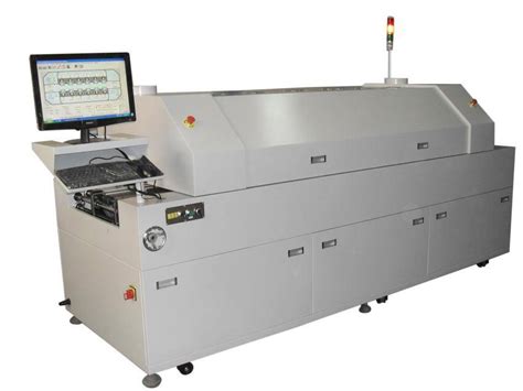
Reflow Soldering Equipment
Reflow soldering requires specific equipment to achieve optimal results:
-
Solder Paste Printer: A solder paste printer is used to apply solder paste onto the PCB. It uses a stencil or screen to deposit the solder paste precisely on the desired areas of the board.
-
Pick-and-Place Machine: An automated pick-and-place machine is used to place components onto the PCB with high speed and accuracy. These machines can handle a wide range of component sizes and types.
-
Reflow Oven: A reflow oven is the core equipment in the reflow soldering process. It consists of multiple heating zones that follow a predetermined temperature profile to melt the solder and create permanent connections between the components and the PCB.
-
Inspection Equipment: Inspection equipment, such as automated optical inspection (AOI) systems or X-ray inspection machines, is used to verify the quality and integrity of the solder joints after the reflow process.
Reflow Soldering Temperature Profile
The reflow soldering temperature profile is a critical factor in achieving reliable solder joints. A typical reflow profile consists of four stages:
-
Preheat: The preheat stage slowly raises the temperature of the PCB and components to activate the flux and remove moisture. The preheat rate is typically around 2-3°C per second, and the preheat temperature ranges from 150-180°C.
-
Soak: The soak stage maintains a constant temperature to ensure that all components and the PCB reach thermal equilibrium. This stage helps to minimize thermal shock and reduce the risk of component damage. The soak temperature is usually between 150-180°C and lasts for 60-120 seconds.
-
Reflow: During the reflow stage, the temperature is increased to the melting point of the solder, typically around 220-250°C for lead-free solder. The peak temperature is maintained for a short duration, usually 30-90 seconds, to allow the solder to melt and form reliable connections.
-
Cooling: The cooling stage gradually lowers the temperature of the PCB and components to allow the molten solder to solidify. The cooling rate should be controlled to prevent thermal shock and ensure the formation of strong solder joints. The cooling rate is typically around 2-4°C per second.
The specific temperature profile parameters may vary depending on the solder paste used, the size and type of components, and the PCB material. It is important to follow the recommended profile provided by the solder paste manufacturer and fine-tune it based on the specific application requirements.
Reflow Soldering vs. Wave Soldering
Reflow soldering and wave soldering are two commonly used soldering methods in the electronics industry. While both techniques aim to create electrical connections between components and the PCB, they differ in their approach and suitability for different applications.
| Characteristic | Reflow Soldering | Wave Soldering |
|---|---|---|
| Soldering Method | Solder paste is applied to the PCB, components are placed, and the assembly is heated in a reflow oven to melt the solder. | The PCB is passed over a molten solder wave, which creates solder joints on the bottom side of the board. |
| Component Types | Suitable for surface mount devices (SMDs) and some through-hole components. | Primarily used for through-hole components, but can also accommodate some SMDs. |
| PCB Orientation | Components are placed on the top side of the PCB. | Components are inserted from the top side of the PCB, and soldering occurs on the bottom side. |
| Thermal Stress | Lower thermal stress on components and PCB due to gradual heating and cooling cycles. | Higher thermal stress on components and PCB due to direct contact with the molten solder wave. |
| Process Control | Precise control over the temperature profile and solder joint formation. | Less control over the solder joint formation, as it depends on the solder wave characteristics. |
| Flux Application | Flux is included in the solder paste. | Separate flux application is required before the soldering process. |
| Throughput | Higher throughput due to the ability to solder multiple components simultaneously. | Lower throughput compared to reflow soldering, as components are soldered sequentially. |
The choice between reflow soldering and wave soldering depends on various factors, such as the type of components used, the PCB design, the production volume, and the specific manufacturing requirements. In many cases, a combination of both methods may be used to assemble a complete PCB.
Frequently Asked Questions (FAQ)
- What is the purpose of flux in reflow soldering?
-
Flux serves several purposes in reflow soldering. It helps to remove oxides and impurities from the surfaces of the components and PCB pads, promoting better solder wetting and joint formation. Flux also protects the surfaces from oxidation during the soldering process and improves the flow characteristics of the molten solder.
-
Can reflow soldering be used for through-hole components?
-
While reflow soldering is primarily used for surface mount devices (SMDs), it can also be used for some through-hole components. However, the process may require additional steps, such as pre-soldering the component leads or using special solder paste formulations. In general, wave soldering is more commonly used for through-hole components.
-
What is the typical temperature range for reflow soldering?
-
The typical temperature range for reflow soldering depends on the type of solder paste used. For lead-free solder, the peak temperature is usually around 240-250°C, while for leaded solder, the peak temperature is around 220-230°C. The exact temperature profile may vary based on the specific solder paste and the recommendations of the manufacturer.
-
How can solder bridging be prevented in reflow soldering?
-
Solder bridging can be prevented by ensuring proper solder paste application, using an appropriate stencil design, and optimizing the reflow temperature profile. Additionally, proper component placement and spacing on the PCB can help minimize the risk of solder bridging. Conducting regular maintenance and calibration of the solder paste printer and pick-and-place machine can also contribute to reducing solder bridging occurrences.
-
What is the role of nitrogen in reflow soldering?
- Nitrogen is sometimes used in reflow soldering to create an inert atmosphere inside the reflow oven. The nitrogen atmosphere helps to reduce oxidation on the surfaces of the components and PCB during the soldering process. This can lead to improved solder joint quality, reduced defects, and enhanced the appearance of the solder joints. However, the use of nitrogen is not always necessary and depends on the specific manufacturing requirements and the desired level of solder joint quality.
In conclusion, reflow soldering is a widely used soldering method in the electronics industry, offering advantages such as high throughput, consistency, and compatibility with surface mount technology. By understanding the reflow soldering process, temperature profile, and common defects, manufacturers can optimize their assembly processes and achieve reliable and high-quality solder joints. While reflow soldering is not suitable for all components and PCB designs, it remains a critical technique in the production of modern electronic devices.


Leave a Reply