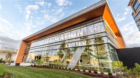
Introduction to Tech Etch Innovation Center
The Tech Etch Innovation Center is a state-of-the-art facility that provides a comprehensive range of services for the design and manufacturing of printed circuit board (PCB) products and parts. As a one-stop destination, the center offers a streamlined process for clients to bring their ideas to life, from concept to production. With a team of experienced engineers, designers, and technicians, the Tech Etch Innovation Center is equipped to handle projects of all sizes and complexities.
Services Offered at Tech Etch Innovation Center
The Tech Etch Innovation Center offers a wide array of services to meet the diverse needs of its clients. These services include:
- PCB Design and Layout
- Prototyping and Small-Batch Production
- Full-Scale Manufacturing
- Quality Control and Testing
- Assembly and Packaging
- Consulting and Technical Support
By providing these services under one roof, the Tech Etch Innovation Center eliminates the need for clients to coordinate with multiple vendors, saving time and reducing the risk of miscommunication.
PCB Design and Layout Services
The Tech Etch Innovation Center’s team of experienced PCB designers and engineers works closely with clients to create custom PCB layouts that meet their specific requirements. Using the latest software and tools, the team can design PCBs for a variety of applications, including:
- Consumer Electronics
- Medical Devices
- Automotive Components
- Industrial Equipment
- Aerospace and Defense Systems
The design process begins with a thorough understanding of the client’s needs and specifications. The team then creates a detailed schematic and layout, taking into account factors such as component placement, signal integrity, and manufacturability. Clients are involved throughout the design process, with regular reviews and feedback sessions to ensure that the final product meets their expectations.
Benefits of Custom PCB Design
Custom PCB design offers several advantages over off-the-shelf solutions:
- Optimized Performance: Custom PCBs can be designed to meet specific performance requirements, such as high-speed signaling or low power consumption.
- Reduced Size and Weight: By designing a PCB specifically for a particular application, the size and weight of the final product can be minimized.
- Cost Savings: Custom PCBs can be designed to use fewer components or less expensive materials, reducing overall costs.
- Improved Reliability: Custom PCBs can be designed with redundancy and fail-safe features to improve reliability and reduce the risk of failure.

Prototyping and Small-Batch Production
Once the PCB design is finalized, the Tech Etch Innovation Center can quickly produce prototypes and small batches for testing and evaluation. The center’s rapid prototyping capabilities allow clients to iterate on their designs and make necessary adjustments before committing to full-scale production.
Prototype PCB Manufacturing Process
The prototype PCB manufacturing process typically involves the following steps:
- PCB Fabrication: The PCB design files are used to create a physical PCB, either through traditional subtractive methods or newer additive processes.
- Component Sourcing: The necessary components are sourced from trusted suppliers, ensuring high quality and availability.
- PCB Assembly: The components are mounted onto the PCB using automated pick-and-place machines or manual soldering, depending on the complexity and quantity of the prototype.
- Testing and Inspection: The assembled PCB is thoroughly tested and inspected to ensure proper functionality and adherence to specifications.
Benefits of Rapid Prototyping
Rapid prototyping offers several benefits for PCB product development:
- Faster Time-to-Market: By quickly producing prototypes, clients can test and refine their designs faster, reducing the overall time-to-market for their products.
- Reduced Risk: Prototyping allows clients to identify and address potential issues early in the development process, reducing the risk of costly mistakes later on.
- Improved Design Iterations: Rapid prototyping enables clients to experiment with different design options and make informed decisions based on real-world testing and feedback.

Full-Scale PCB Manufacturing
Once the prototype has been approved, the Tech Etch Innovation Center can seamlessly transition to full-scale production. The center’s manufacturing capabilities include:
- High-Volume PCB Fabrication
- Automated PCB Assembly
- Box Build and System Integration
- Conformal Coating and Potting
- Cable and Wire Harness Assembly
The Tech Etch Innovation Center’s manufacturing processes are optimized for efficiency, quality, and cost-effectiveness. The center’s team of experienced technicians and engineers oversees every aspect of production, from material sourcing to final inspection.
PCB Manufacturing Process Flow
The PCB manufacturing process typically follows these steps:
- Material Preparation: The raw materials, such as copper-clad laminates and prepregs, are cut to size and cleaned.
- Imaging and Etching: The PCB design is transferred onto the copper layer using photolithography, and the unwanted copper is etched away.
- Drilling and Plating: Holes are drilled into the PCB for component placement, and the holes are plated with copper to create electrical connections.
- Solder Mask and Silkscreen: A solder mask is applied to protect the copper traces, and a silkscreen layer is added for component labeling and identification.
- Surface Finish: A surface finish, such as HASL or ENIG, is applied to the exposed copper to improve solderability and protect against oxidation.
- Electrical Testing: The finished PCB is tested for continuity, insulation resistance, and other electrical properties to ensure proper functionality.
Benefits of Outsourcing PCB Manufacturing
Outsourcing PCB manufacturing to a facility like the Tech Etch Innovation Center offers several advantages:
- Cost Savings: By leveraging the center’s economies of scale and purchasing power, clients can reduce their manufacturing costs compared to in-house production.
- Access to Expertise: The Tech Etch Innovation Center’s team of experienced professionals can provide valuable guidance and support throughout the manufacturing process.
- Scalability: The center’s manufacturing capabilities can easily scale up or down to meet changing demand, allowing clients to respond quickly to market conditions.
- Quality Assurance: The Tech Etch Innovation Center’s rigorous quality control processes ensure that every PCB meets the highest standards of reliability and performance.

Quality Control and Testing
The Tech Etch Innovation Center places a strong emphasis on quality control and testing to ensure that every PCB product meets or exceeds client expectations. The center’s quality control processes include:
- Incoming Material Inspection
- In-Process Quality Checks
- Automated Optical Inspection (AOI)
- X-Ray Inspection
- Functional Testing
- Environmental Testing
By implementing these quality control measures at every stage of production, the Tech Etch Innovation Center can identify and address potential issues before they impact the final product.
Common PCB Testing Methods
Some of the most common PCB testing methods used at the Tech Etch Innovation Center include:
| Testing Method | Description | Purpose |
|---|---|---|
| In-Circuit Testing (ICT) | Electrical testing of individual components and circuits | Identify manufacturing defects and component failures |
| Flying Probe Testing | Precise electrical testing using movable probes | Test specific points on the PCB without the need for a custom fixture |
| Boundary Scan Testing | Testing of digital components using built-in test access ports | Identify faults in components, interconnects, and printed circuits |
| Functional Testing | Testing of the PCB’s overall functionality and performance | Ensure that the PCB meets the desired specifications and requirements |
By using a combination of these testing methods, the Tech Etch Innovation Center can provide a comprehensive quality assurance process that minimizes the risk of defects and failures.
Assembly and Packaging Services
In addition to PCB design and manufacturing, the Tech Etch Innovation Center offers assembly and packaging services to help clients bring their products to market. These services include:
- Component Sourcing and Procurement
- PCB Assembly (Through-Hole and Surface Mount)
- Box Build and System Integration
- Cable and Wire Harness Assembly
- Custom Packaging and Labeling
By providing these services, the Tech Etch Innovation Center can help clients streamline their supply chain and reduce the time and costs associated with managing multiple vendors.
Benefits of Turnkey PCB Assembly
Turnkey PCB assembly, where a single vendor handles all aspects of PCB production from design to final assembly, offers several benefits:
- Simplified Supply Chain: By working with a single vendor, clients can reduce the complexity of their supply chain and minimize the risk of delays or miscommunications.
- Faster Time-to-Market: Turnkey assembly can help clients bring their products to market faster by eliminating the need to coordinate between multiple vendors.
- Cost Savings: By bundling services, turnkey assembly providers can often offer lower costs compared to working with multiple vendors.
- Improved Quality Control: Turnkey assembly allows for better control over the entire production process, ensuring consistent quality from start to finish.
Consulting and Technical Support
The Tech Etch Innovation Center’s team of experienced engineers and technicians is available to provide consulting and technical support services to clients throughout the PCB development process. These services can help clients:
- Optimize PCB designs for manufacturability and cost-effectiveness
- Select the best materials and components for their application
- Troubleshoot problems and identify root causes
- Develop and implement process improvements
- Navigate regulatory requirements and industry standards
By leveraging the expertise of the Tech Etch Innovation Center’s team, clients can overcome challenges and achieve their goals more efficiently and effectively.
Benefits of Expert Consulting and Technical Support
Expert consulting and technical support can provide several benefits for PCB product development:
- Improved Design Quality: By working with experienced professionals, clients can improve the quality and reliability of their PCB designs.
- Faster Problem Resolution: Expert support can help clients quickly identify and resolve problems, minimizing downtime and delays.
- Access to Industry Knowledge: Consulting services can provide clients with valuable insights into industry trends, best practices, and emerging technologies.
- Risk Mitigation: By leveraging expert guidance, clients can reduce the risk of costly mistakes and ensure compliance with relevant standards and regulations.
FAQs
-
What types of PCB products and parts can the Tech Etch Innovation Center design and manufacture?
The Tech Etch Innovation Center can design and manufacture a wide range of PCB products and parts, including rigid PCBs, flexible PCBs, rigid-flex PCBs, and high-density interconnects (HDIs). The center serves clients in various industries, such as consumer electronics, medical devices, automotive, aerospace, and defense. -
What is the typical lead time for PCB Prototyping and production at the Tech Etch Innovation Center?
Lead times for PCB prototyping and production can vary depending on the complexity of the design, the materials required, and the quantity ordered. However, the Tech Etch Innovation Center’s streamlined processes and rapid prototyping capabilities can often deliver prototypes within days and production orders within weeks. -
What certifications and quality standards does the Tech Etch Innovation Center maintain?
The Tech Etch Innovation Center maintains several industry certifications and adheres to strict quality standards, including ISO 9001, ISO 13485, AS9100, and IPC-A-610. These certifications demonstrate the center’s commitment to quality and reliability in PCB design and manufacturing. -
How does the Tech Etch Innovation Center ensure the security and confidentiality of client designs and intellectual property?
The Tech Etch Innovation Center has robust security measures in place to protect client designs and intellectual property. These measures include secure data storage, access controls, non-disclosure agreements, and employee training on confidentiality and data protection. -
What support services are available for clients who need assistance with PCB design or troubleshooting?
The Tech Etch Innovation Center offers a range of support services for clients, including design assistance, material selection guidance, manufacturability analysis, and troubleshooting support. The center’s team of experienced engineers and technicians is available to provide expert guidance and support throughout the PCB development process.
Conclusion
The Tech Etch Innovation Center is a comprehensive resource for clients seeking a one-stop destination for PCB product and part design and manufacturing. With its state-of-the-art facilities, experienced team, and commitment to quality and innovation, the center is well-equipped to help clients bring their ideas to life efficiently and cost-effectively.
By offering a full range of services, from design and prototyping to full-scale production and assembly, the Tech Etch Innovation Center can streamline the PCB development process and help clients achieve their goals faster and with fewer challenges. Whether clients need assistance with a simple prototype or a complex, high-volume production run, the Tech Etch Innovation Center has the expertise and capabilities to deliver results.
As the demand for high-quality, reliable PCBs continues to grow across industries, the Tech Etch Innovation Center is poised to be a valuable partner for companies looking to innovate and succeed in today’s competitive market.


Leave a Reply