Introduction to Gerber Files
Gerber files are the standard file format used in the printed circuit board (PCB) industry for the design and manufacture of PCBs. They contain all the necessary information required to fabricate a PCB, including the copper layers, solder mask, silkscreen, and drill data. Gerber files are essential for communicating the PCB design to the manufacturing facility, ensuring that the final product meets the desired specifications.
In this comprehensive guide, we will walk you through the process of generating Gerber files step by step. We will cover the following topics:
- Understanding the Gerber file format
- Setting up your PCB design software for Gerber File Generation
- Generating individual layer files
- Creating the drill file
- Reviewing and verifying your Gerber files
- Exporting and sending your Gerber files to the manufacturer
By the end of this guide, you will have a solid understanding of how to generate Gerber files for your PCB designs, ensuring a smooth transition from design to manufacturing.
Understanding the Gerber File Format
What is the Gerber File Format?
The Gerber file format, also known as RS-274X, is a standard file format used to describe the printed circuit board images. It was developed by the Gerber Systems Corp., which is now a subsidiary of Ucamco. The format has evolved over time, with the current version being the Extended Gerber or X2 format.
Gerber files are ASCII text files that contain a series of commands and coordinates that describe the various layers of a PCB. Each layer of the PCB, such as the copper layers, solder mask, and silkscreen, is represented by a separate Gerber file.
Layers in a Gerber File
A typical PCB design consists of several layers, each represented by a separate Gerber file. The most common layers include:
- Top Copper (GTL): The top copper layer of the PCB, containing traces and pads.
- Bottom Copper (GBL): The bottom copper layer of the PCB, containing traces and pads.
- Top Soldermask (GTS): The top solder mask layer, which protects the copper traces and pads from oxidation and prevents solder bridges.
- Bottom Soldermask (GBS): The bottom solder mask layer, serving the same purpose as the top solder mask.
- Top Silkscreen (GTO): The top silkscreen layer, containing text and symbols for component placement and identification.
- Bottom Silkscreen (GBO): The bottom silkscreen layer, containing text and symbols for component placement and identification.
- Drill File (DRL): The drill file contains information about the holes to be drilled in the PCB, including their sizes and locations.
Additional layers may be included depending on the complexity of the PCB design, such as inner copper layers, paste mask layers, and outline layers.
Apertures and D-Codes
Gerber files use apertures to define the shapes and sizes of the features on each layer. Apertures are described using D-Codes, which are numerical identifiers that correspond to specific shapes and sizes. For example, D10 may represent a circular aperture with a diameter of 0.5mm, while D11 may represent a rectangular aperture with dimensions of 1mm x 2mm.
The aperture information is typically stored in a separate file called an aperture list or a wheel file. This file defines the D-Codes used in the Gerber files and their corresponding shapes and sizes.

Setting Up Your PCB Design Software for Gerber File Generation
To generate Gerber files, you will need to use a PCB design software package. Some popular options include:
- Altium Designer
- KiCad
- Eagle
- OrCAD
- Cadence Allegro
Each software package has its own process for generating Gerber files, but the general principles remain the same. In this guide, we will use Altium Designer as an example, but the steps can be adapted to other software packages.
Configuring the CAM Processor
Before generating Gerber files, you need to configure the CAM (Computer-Aided Manufacturing) processor in your PCB design software. The CAM processor is responsible for converting the PCB design data into the Gerber file format.
In Altium Designer, you can access the CAM processor by following these steps:
- Open your PCB design project.
- Click on the “File” menu and select “Fabrication Outputs” > “Gerber Files”.
- The CAM processor window will open, displaying the available layers and settings.
Setting Up the Gerber File Outputs
In the CAM processor window, you will need to set up the Gerber file outputs for each layer of your PCB. This involves selecting the appropriate layer, choosing the Gerber file format, and specifying the output directory.
To set up the Gerber file outputs in Altium Designer:
- In the CAM processor window, click on the “Layers” tab.
- Select the desired layer from the list, such as “Top Copper” or “Bottom Soldermask”.
- In the “Output” section, choose “Gerber” as the format.
- Specify the output directory where the Gerber files will be saved.
- Repeat steps 2-4 for each layer of your PCB.
Configuring the Drill File Output
In addition to the Gerber files for each layer, you also need to generate a drill file that contains information about the holes to be drilled in the PCB.
To set up the drill file output in Altium Designer:
- In the CAM processor window, click on the “Drill Drawing” tab.
- Select the “Drill Drawing” layer from the list.
- In the “Output” section, choose “Excellon” as the format.
- Specify the output directory where the drill file will be saved.

Generating Individual Layer Files
With the CAM processor configured, you can now generate the individual Gerber files for each layer of your PCB.
Generating Copper Layer Files
To generate the Gerber files for the copper layers (e.g., Top Copper and Bottom Copper):
- In the CAM processor window, select the desired copper layer from the “Layers” tab.
- Click on the “Process Job” button to generate the Gerber file.
- The Gerber file will be saved in the specified output directory.
- Repeat steps 1-3 for each copper layer in your PCB design.
Generating Solder Mask Layer Files
To generate the Gerber files for the solder mask layers (e.g., Top Soldermask and Bottom Soldermask):
- In the CAM processor window, select the desired solder mask layer from the “Layers” tab.
- Click on the “Process Job” button to generate the Gerber file.
- The Gerber file will be saved in the specified output directory.
- Repeat steps 1-3 for each solder mask layer in your PCB design.
Generating Silkscreen Layer Files
To generate the Gerber files for the silkscreen layers (e.g., Top Silkscreen and Bottom Silkscreen):
- In the CAM processor window, select the desired silkscreen layer from the “Layers” tab.
- Click on the “Process Job” button to generate the Gerber file.
- The Gerber file will be saved in the specified output directory.
- Repeat steps 1-3 for each silkscreen layer in your PCB design.

Creating the Drill File
The drill file contains information about the holes to be drilled in the PCB, including their sizes and locations. To generate the drill file:
- In the CAM processor window, click on the “Drill Drawing” tab.
- Select the “Drill Drawing” layer from the list.
- Click on the “Process Job” button to generate the drill file.
- The drill file will be saved in the specified output directory.
Reviewing and Verifying Your Gerber Files
Before sending your Gerber files to the manufacturer, it is crucial to review and verify them to ensure that they accurately represent your PCB design. This step helps to catch any errors or discrepancies that may cause issues during the manufacturing process.
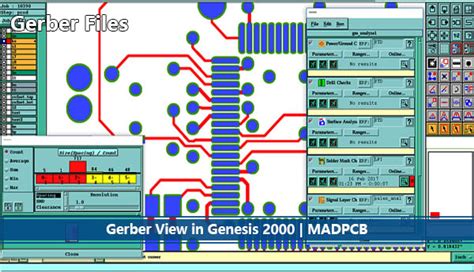
Visually Inspecting the Gerber Files
To visually inspect your Gerber files:
- Open the Gerber files in a Gerber viewer software, such as GC-Prevue or ViewMate.
- Carefully examine each layer, looking for any missing or incorrect features, such as traces, pads, or holes.
- Check the alignment of the layers to ensure that they match up correctly.
- Verify that the dimensions and sizes of the features are accurate and consistent with your PCB design.
Running a Design Rule Check (DRC)
Most PCB design software packages include a Design Rule Check (DRC) feature that helps to identify potential issues in your PCB design. Running a DRC on your Gerber files can help to catch any design rule violations or inconsistencies.
To run a DRC in Altium Designer:
- Open your PCB design project.
- Click on the “Tools” menu and select “Design Rule Check”.
- In the DRC window, select the appropriate rule set for your PCB design.
- Click on the “Run Design Rule Check” button to start the DRC process.
- Review the DRC report and address any issues flagged by the software.
Comparing Gerber Files to the Original PCB Design
As a final verification step, compare your generated Gerber files to the original PCB design to ensure that they match. This can be done by overlaying the Gerber files on top of the PCB design in your PCB design software.
In Altium Designer:
- Open your PCB design project.
- Click on the “File” menu and select “Import” > “Gerber”.
- Select the Gerber files you want to import and click “Open”.
- The imported Gerber files will be overlaid on top of your PCB design.
- Visually compare the Gerber files to the original design, checking for any discrepancies or misalignments.
Exporting and Sending Your Gerber Files to the Manufacturer
Once you have reviewed and verified your Gerber files, you are ready to export and send them to your PCB manufacturer.
Exporting Gerber Files
To export your Gerber files:
- Open your PCB design project.
- Click on the “File” menu and select “Fabrication Outputs” > “Gerber Files”.
- In the CAM processor window, click on the “Output” tab.
- Click on the “Process Job” button to generate the Gerber files.
- The Gerber files will be saved in the specified output directory.
Compressing and Sending Gerber Files
Most PCB manufacturers prefer to receive Gerber files in a compressed format, such as ZIP or RAR. To compress your Gerber files:
- Navigate to the output directory where your Gerber files are saved.
- Select all the Gerber files, including the drill file.
- Right-click on the selected files and choose “Send to” > “Compressed (zipped) folder”.
- The compressed file will be created in the same directory.
To send your Gerber files to the manufacturer:
- Follow the manufacturer’s specific instructions for submitting Gerber files. This may involve uploading the files to their website, emailing them, or using a dedicated PCB Ordering platform.
- Provide any additional information required by the manufacturer, such as PCB specifications, quantity, and delivery requirements.
- Double-check that you have sent the correct files before submitting your order.
Common Gerber File Generation Issues and Solutions
| Problem | Solution |
|---|---|
| Incorrect layer alignment | Ensure that the layer stackup and alignment settings are correct in your PCB design software. Use a Gerber viewer to visually inspect the alignment of the layers. |
| Missing or incorrect features | Review your PCB design for any missing or incorrect features, such as traces, pads, or holes. Run a Design Rule Check (DRC) to identify potential issues. |
| Incorrect aperture sizes | Verify that the aperture sizes specified in the Gerber files match your PCB design. Check the aperture list or wheel file for accuracy. |
| Incorrect drill file | Ensure that the drill file includes all the necessary holes and that their sizes and locations are accurate. Compare the drill file to the original PCB design. |
| Incorrect file naming | Follow the manufacturer’s guidelines for naming your Gerber files. Use a consistent and descriptive naming convention to avoid confusion. |
Gerber File Generation FAQs
-
What is the difference between Gerber files and drill files?
Gerber files contain information about the copper layers, solder mask, and silkscreen of a PCB, while drill files contain information about the holes to be drilled in the PCB, including their sizes and locations. -
Can I generate Gerber files from any PCB design software?
Most PCB design software packages, such as Altium Designer, KiCad, and Eagle, have built-in features for generating Gerber files. However, the specific steps and settings may vary between software packages. -
How do I know if my Gerber files are correct?
To verify the accuracy of your Gerber files, visually inspect them using a Gerber viewer, run a Design Rule Check (DRC), and compare them to the original PCB design. Look for any missing or incorrect features, alignment issues, or inconsistencies. -
What should I do if my Gerber files are rejected by the manufacturer?
If your Gerber files are rejected by the manufacturer, ask for specific feedback on the issues they encountered. Review and correct your Gerber files based on their feedback, and resubmit them for fabrication. -
Can I modify Gerber files directly?
While it is possible to modify Gerber files directly using a text editor, it is not recommended. Gerber files are complex and prone to errors if edited manually. Instead, make any necessary changes in your PCB design software and regenerate the Gerber files.
Conclusion
Generating accurate Gerber files is essential for the successful fabrication of your PCB design. By following the step-by-step guide provided in this article, you can ensure that your Gerber files are correctly generated, reviewed, and verified before sending them to the manufacturer.
Key points to remember:
- Set up your PCB design software’s CAM processor to generate Gerber files for each layer of your PCB.
- Generate individual Gerber files for the copper layers, solder mask layers, and silkscreen layers.
- Create the drill file containing information about the holes to be drilled in the PCB.
- Review and verify your Gerber files using visual inspection, Design Rule Checks (DRC), and comparison to the original PCB design.
- Export your Gerber files, compress them, and send them to the manufacturer according to their specific guidelines.
By understanding the Gerber file format, setting up your PCB design software correctly, and following best practices for Gerber file generation, you can streamline the PCB fabrication process and ensure the successful manufacture of your PCB designs.


Leave a Reply