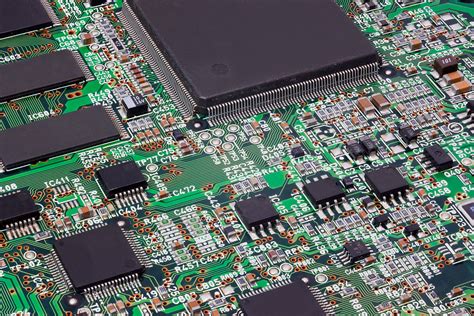
Introduction to PCBA Manufacturing
PCBA (Printed Circuit Board Assembly) manufacturing is the process of assembling electronic components onto a printed circuit board (PCB) to create a functional electronic device. The process involves several steps, including PCB design, component sourcing, assembly, testing, and packaging. In this comprehensive guide, we will walk you through each step of the PCBA manufacturing process, providing insights and best practices to ensure a successful outcome.
The Importance of PCBA Manufacturing
PCBA manufacturing plays a crucial role in the production of electronic devices across various industries, such as:
- Consumer electronics
- Automotive
- Medical devices
- Aerospace and defense
- Industrial automation
The quality and reliability of the PCBA directly impact the performance and longevity of the final product. Therefore, it is essential to understand and optimize each step of the PCBA manufacturing process.

Step 1: PCB Design and Fabrication
PCB Design Considerations
Before starting the PCBA manufacturing process, it is crucial to have a well-designed PCB. The PCB design should take into account factors such as:
- Component placement and routing
- Signal integrity
- Thermal management
- Electromagnetic compatibility (EMC)
- Manufacturing constraints
PCB Fabrication Process
Once the PCB design is finalized, the next step is to fabricate the bare PCB. The PCB fabrication process typically involves the following sub-steps:
- Substrate preparation
- Copper foil lamination
- Photoresist application
- Exposure and development
- Etching
- Soldermask application
- Silkscreen printing
- Surface finish application
- Electrical testing

Step 2: Component Sourcing and Management
Component Selection
Selecting the right components for your PCBA is crucial for ensuring the desired functionality, reliability, and cost-effectiveness of the final product. When selecting components, consider factors such as:
- Functionality and performance
- Quality and reliability
- Availability and lead time
- Cost
- Compliance with industry standards and regulations
Component Management
Effective component management is essential for streamlining the PCBA manufacturing process and avoiding delays or disruptions. Some best practices for component management include:
- Maintaining an accurate and up-to-date bill of materials (BOM)
- Establishing reliable supply chain partnerships
- Implementing inventory management systems
- Conducting regular quality inspections and audits

Step 3: PCB Assembly
Surface Mount Technology (SMT) Assembly
SMT assembly is the most common method for mounting components onto a PCB. The process involves the following sub-steps:
- Solder paste printing
- Component placement
- Reflow soldering
- Inspection and repair
Through-Hole Technology (THT) Assembly
THT assembly is used for larger components or those that require higher mechanical strength. The process involves the following sub-steps:
- Component insertion
- Wave soldering or selective soldering
- Inspection and repair
Automated Optical Inspection (AOI)
AOI is a crucial step in the PCBA manufacturing process, as it helps identify and correct any defects or issues before the board moves on to the next stage. AOI systems use high-resolution cameras and advanced algorithms to detect:
- Component presence and placement
- Solder joint quality
- Polarity and orientation
- Dimensional accuracy
Step 4: Testing and Quality Control
In-Circuit Testing (ICT)
ICT is a method for testing the functionality and connectivity of individual components on the PCBA. This is typically done using a bed-of-nails fixture that makes contact with specific test points on the board.
Functional Testing
Functional testing involves verifying the overall performance and functionality of the assembled PCBA. This may include:
- Power-on testing
- Boundary scan testing
- System-level testing
- Environmental testing (e.g., temperature, humidity, vibration)
Quality Control and Assurance
Implementing a robust quality control and assurance program is essential for ensuring the consistency and reliability of your PCBA manufacturing process. This may involve:
- Establishing and maintaining quality standards and procedures
- Conducting regular process audits and improvements
- Implementing statistical process control (SPC) methods
- Providing adequate training and resources for personnel
Step 5: Conformal Coating and Potting
Conformal Coating
Conformal coating is a protective layer applied to the PCBA to shield it from environmental factors such as moisture, dust, and chemicals. Common conformal coating materials include:
- Acrylic
- Silicone
- Polyurethane
- Epoxy
Potting
Potting involves encapsulating the PCBA in a solid compound, such as epoxy or silicone, to provide additional protection against mechanical stress, shock, and vibration. Potting is often used in applications where the PCBA is exposed to harsh environments or extreme conditions.
Step 6: Final Assembly and Packaging
Final Assembly
The final assembly stage involves integrating the PCBA into the finished product, along with any other necessary components, such as displays, batteries, or enclosures. This stage may also include additional testing and quality control measures to ensure the product meets all specified requirements.
Packaging and Shipping
Proper packaging is essential for protecting the PCBA and the finished product during storage and transportation. Some best practices for packaging include:
- Using anti-static materials to prevent electrostatic discharge (ESD) damage
- Employing moisture barrier bags or desiccants to control humidity
- Utilizing appropriate cushioning and bracing to minimize shock and vibration
- Labeling packages clearly with handling and storage instructions
Frequently Asked Questions (FAQ)
1. What is the difference between PCB and PCBA?
A PCB (Printed Circuit Board) is the bare board without any components attached, while a PCBA (Printed Circuit Board Assembly) is a PCB with all the necessary electronic components soldered onto it, making it a functional Electronic Assembly.
2. What are the most common defects in PCBA manufacturing?
Common defects in PCBA manufacturing include solder bridge, tombstoning, component shift, insufficient or excessive solder, and component misalignment. These defects can be minimized through proper process control, inspection, and quality assurance measures.
3. How can I ensure the reliability and longevity of my PCBA?
To ensure the reliability and longevity of your PCBA, consider the following factors:
- Proper PCB design and component selection
- Robust manufacturing processes and quality control
- Adequate protection against environmental factors (e.g., conformal coating, potting)
- Thorough testing and validation
- Ongoing monitoring and maintenance
4. What are the benefits of outsourcing PCBA manufacturing?
Outsourcing PCBA manufacturing can offer several benefits, including:
- Access to specialized expertise and state-of-the-art equipment
- Reduced capital investment and overhead costs
- Improved scalability and flexibility
- Faster time-to-market
- Enhanced focus on core competencies
5. How do I choose the right PCBA manufacturing partner?
When selecting a PCBA manufacturing partner, consider the following factors:
- Technical capabilities and experience
- Quality control and assurance processes
- Capacity and scalability
- Communication and responsiveness
- Intellectual property (IP) protection
- Cost and delivery performance
- References and reputation in the industry
Conclusion
PCBA manufacturing is a complex and multi-faceted process that requires careful planning, execution, and quality control. By understanding and optimizing each step of the process, from PCB design to final assembly and packaging, you can ensure the successful production of high-quality, reliable electronic products.
When embarking on a PCBA manufacturing project, it is essential to work with experienced and reputable partners who can provide the necessary expertise, resources, and support to help you achieve your goals. By following the best practices and guidelines outlined in this article, you can navigate the challenges of PCBA manufacturing and bring your electronic product vision to life.
| Step | Key Considerations |
|---|---|
| 1. PCB Design and Fabrication | – Component placement and routing – Signal integrity – Thermal management – Manufacturing constraints |
| 2. Component Sourcing and Management | – Functionality and performance – Quality and reliability – Availability and lead time – Cost |
| 3. PCB Assembly | – SMT assembly – THT assembly – Automated optical inspection (AOI) |
| 4. Testing and Quality Control | – In-circuit testing (ICT) – Functional testing – Quality control and assurance |
| 5. Conformal Coating and Potting | – Conformal coating materials – Potting compounds and applications |
| 6. Final Assembly and Packaging | – Integration with finished product – Packaging materials and methods – Labeling and shipping |


Leave a Reply