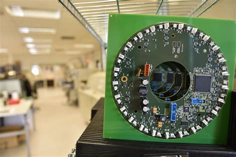
What is SMT PCB Assembly?
SMT (Surface Mount Technology) PCB (Printed Circuit Board) assembly is the process of attaching electronic components directly onto the surface of a printed circuit board. This is in contrast to through-hole technology, where component leads are inserted into holes drilled in the PCB and soldered to pads on the opposite side.
SMT has largely replaced through-hole technology in PCB manufacturing due to several advantages:
- Smaller component sizes allow for denser boards
- Components can be placed on both sides of the board
- Faster and more automated assembly
- Lower production costs for high volume
- Better mechanical performance under shake and vibration
The basic SMT assembly process involves:
1. Solder paste printing
2. Component placement
3. Reflow soldering
Advantages of SMT over Through-Hole
| Aspect | Through-Hole | SMT |
|---|---|---|
| Component Size | Larger | Smaller |
| Component Placement | One side only | Both sides |
| Density | Lower | Higher |
| Assembly | More manual | More automated |
| Production Cost | Higher for volume | Lower for volume |
| Mechanical Strength | Lower | Higher |
SMT PCB Assembly Process
Step 1: Solder Paste Printing
The first step in SMT assembly is to print solder paste onto the PCB’s pads where components will be placed. Solder paste is a mixture of tiny solder balls and flux. It’s a sticky gray material with the consistency of toothpaste.
The solder paste is applied using a stainless steel or nickel stencil. The stencil has laser-cut openings that match the pads on the PCB. It’s placed over the PCB and aligned precisely. Then solder paste is spread over the stencil with a squeegee blade, forcing it through the openings and onto the pads.
Solder paste printing is usually done by automated stencil printing machines. Key factors in getting a good print are the stencil design, paste viscosity, squeegee pressure and speed, and board support.
Step 2: Component Placement
After the solder paste is printed, the PCB moves on to the pick-and-place machine for component placement. This machine uses a vacuum nozzle or gripper to pick up components from feeders or trays and place them onto their respective pads on the PCB with high speed and precision.
Modern pick-and-place machines are extremely fast and accurate. High-end machines can place over 100,000 components per hour with placement accuracy of ±0.025 mm. The machine is programmed with the coordinates of each component on the PCB along with the rotation. Advanced machines have multiple nozzles and can place a variety of component types and sizes.
The components are held in place temporarily by the stickiness of the solder paste. Proper paste volume is important – too little and the component may not stay in place, too much and it could cause bridging between pads.
Step 3: Reflow Soldering
With all the components placed, the PCB is ready for reflow soldering. This is done in a reflow oven, which heats the entire board in a controlled way to melt the solder paste and permanently attach the components.
The reflow process involves several stages:
-
Preheat: The board is slowly heated to evaporate solvents and activate the flux. This prepares the solder paste for reflow.
-
Soak: The temperature is held steady to allow the entire board to reach an even temperature. This prevents thermal stress.
-
Reflow: The temperature is ramped up quickly to the melting point of the solder (usually around 220°C for lead-free solder). The solder paste melts, forming solder joints between the component leads and the pads. Surface tension causes the molten solder to wick up the leads.
-
Cooling: The board is cooled in a controlled way to solidify the solder joints without causing thermal stress. Fans are often used for faster cooling.
The entire reflow process is controlled by a precise temperature profile that’s specific to the solder paste and PCB design. Getting the profile right is crucial for good solder joint formation and to prevent defects like cold joints, tombstoning, or delamination.
After reflow, the PCB goes through inspection and testing to verify the assembly quality before further processing or shipment.

SMT Component Types and Packages
SMT components come in a wide variety of types and packages. Here are some of the most common:
Passive Components
- Resistors: 0201, 0402, 0603, 0805, 1206, 2010, 2512
- Capacitors: 0201, 0402, 0603, 0805, 1206, 1210
- Inductors: 0603, 0805, 1008, 1206, 1210
The numbers refer to the size in hundredths of an inch – for example, an 0603 package is 0.06″ by 0.03″.
Active Components
- SOT (Small Outline Transistor): SOT-23, SOT-223, SOT-89
- QFP (Quad Flat Pack): TQFP, LQFP, PQFP, ranging from 32 to over 200 pins
- QFN (Quad Flat No-Lead): Ranging from 16 to over 100 pins
- BGA (Ball Grid Array): Ranging from a few dozen to over 1000 solder balls
Integrated Circuits
- SOIC (Small Outline Integrated Circuit): 8 to 28 pins, gullwing leads
- SSOP (Shrink Small Outline Package): Similar to SOIC but smaller
- TSSOP (Thin Shrink Small Outline Package): Even thinner than SSOP

Design Considerations for SMT PCBs
Designing a PCB for SMT assembly requires some specific considerations:
Pad Size and Spacing
Pads need to be the right size for the component leads and have enough space between them to prevent solder bridging. IPC standards provide recommended pad sizes and spacing for different component types.
Solder Mask
Solder mask is a polymer coating applied to the PCB that prevents solder from sticking where it’s not supposed to. Openings in the solder mask define where solder is applied. The solder mask opening should be slightly larger than the pad to allow for some alignment tolerance.
Silk Screen
The silk screen is the white text and symbols printed on the PCB that identify components and show other information. It’s important to make sure the silk screen doesn’t overlap with pads and isn’t too close to components.
Thermal Design
SMT components, especially high-power ones like BGAs, can generate significant heat. The PCB design needs to provide adequate heat sinking and cooling, such as large copper pours, thermal vias, or even heat pipes in extreme cases.
Assembly Considerations
The PCB design should also consider the needs of the assembly process:
- Providing fiducials for machine vision alignment
- Avoiding tall components near the board edges that could interfere with conveyors
- Placing connectors and other hand-placed components in accessible locations
- Allowing space for test points and programming headers

SMT Quality Control and Inspection
Ensuring the quality of SMT assembly involves several stages of inspection and testing:
Visual Inspection
After reflow, the PCBs are visually inspected for obvious defects like missing components, tombstoning, bridging, or misalignment. This is often done with the help of magnification or machine vision systems.
Automated Optical Inspection (AOI)
AOI uses high-resolution cameras and computer vision algorithms to automatically detect assembly defects. It can spot problems that are difficult to see with the naked eye and can inspect boards much faster than manual methods.
X-Ray Inspection
For components like BGAs where the solder joints are hidden under the package, X-ray inspection is used. X-ray systems can see through the component to check for voids, bridges, or misalignment in the solder balls.
In-Circuit Testing (ICT)
ICT uses a bed-of-nails fixture to make electrical contact with test points on the PCB. It can then check for short circuits, open circuits, resistance, capacitance, and basic functionality of the circuit. ICT is good for catching defects that visual methods might miss.
Functional Testing
After assembly, the PCBs usually go through some kind of functional test to verify that they work as intended. This could be as simple as powering on the board and checking for proper voltage levels, or as complex as running the board through its full operation and checking its outputs.
Frequently Asked Questions
What are the most common defects in SMT assembly?
Some of the most common SMT defects are:
- Solder bridges: Unintended solder connections between two pads
- Open joints: Solder joint that isn’t properly formed, causing an open circuit
- Tombstoning: One end of a component lifting off the pad due to uneven heating
- Component shifting: Component moves out of position during reflow
- Insufficient or excessive solder: Too little solder can cause a weak joint, too much can cause bridging
What causes tombstoning in SMT?
Tombstoning happens when one end of a component lifts off the pad during reflow. It’s caused by an imbalance in the surface tension forces pulling on the two ends of the component. This can be due to uneven heating, different sized pads, or uneven solder paste volumes.
How do you prevent solder bridging?
Solder bridging can be prevented by:
- Ensuring proper stencil design and paste printing for the right Solder Volume
- Having adequate spacing between pads
- Controlling the reflow profile to avoid excessive solder splatter
- Using solder mask between pads as a barrier
What’s the difference between lead and lead-free solder?
Leaded solder traditionally used a tin-lead alloy, often Sn63/Pb37 (63% tin, 37% lead). Due to environmental regulations, lead-free solder is now widely used, typically Sn96.5/Ag3.0/Cu0.5 (96.5% tin, 3% silver, 0.5% copper).
Lead-free solder has a higher melting point (217°C vs 183°C for leaded) and requires more precise reflow control. It can also be more prone to certain defects like tin whiskers.
How do you rework an SMT board?
Reworking an SMT board involves selectively removing and replacing components without damaging the board or other components. This is done using specialized tools like hot air rework stations, soldering irons with fine tips, and precision tweezers.
The basic process is:
- Heat up the component to melt the solder
- Lift the component off the board
- Clean the pads of old solder
- Print new solder paste
- Place new component and reflow
Proper technique and experience are important to avoid damage during rework. Some components like large BGAs can be very challenging to rework and may require specialized equipment.
This comprehensive guide has covered the basics of SMT PCB assembly, from the process flow to component types, design considerations, quality control, and common questions. While SMT has revolutionized PCB manufacturing with its efficiency and miniaturization capabilities, it’s also a complex process that requires careful engineering and attention to detail at every step to ensure reliable, high-quality results.


Leave a Reply