What is PCB Fabrication?
PCB fabrication is the process of creating printed circuit boards (PCBs) that are used to mechanically support and electrically connect electronic components. PCBs are essential in all but the simplest electronic devices. The fabrication process involves several steps to create the final board, including:
- Design and layout
- Material selection
- Imaging and etching
- Drilling and plating
- Solder mask application
- Silkscreen printing
- Surface finish application
- Electrical testing
- Cutting and packaging
Each of these steps requires precision and adherence to industry standards to ensure the PCB functions properly in the end application.
PCB Design and Layout
The first step in PCB fabrication is designing the circuit and laying out the components on the board. This is typically done using electronic design automation (EDA) software. The designer must consider factors such as:
- Schematic design
- Component placement
- Trace routing
- Power and ground planes
- Electromagnetic interference (EMI)
- Thermal management
- Manufacturing constraints
Once the design is complete, the EDA software generates output files that are used in the fabrication process, including:
- Gerber files for each layer of the board
- NC drill files for hole locations and sizes
- Bill of materials (BOM) for component purchasing
- Assembly drawings for manufacturing reference

PCB Material Selection
The substrate material of a PCB is typically made of a glass-reinforced epoxy laminate, such as FR-4. The properties of the laminate, including the dielectric constant (Dk) and dissipation factor (Df), affect the electrical performance of the board.
Other common PCB materials include:
| Material | Dk | Df | Applications |
|---|---|---|---|
| Polyimide | 3.5 | 0.002 | High temperature, flexible PCBs |
| Teflon | 2.1 | 0.001 | High frequency, low loss |
| Ceramic | 9.8 | 0.001 | High power, high frequency |
| Aluminum | 1.0 | – | Heat sinking, mechanical strength |
The copper weight of the laminate determines the thickness of the copper traces. Common copper weights are:
- 0.5 oz (17.5 μm)
- 1 oz (35 μm)
- 2 oz (70 μm)
- 3 oz (105 μm)
Thicker copper allows for higher current carrying capacity but increases the cost of the board.

PCB Imaging and Etching
Once the design files are received by the fabrication house, the first manufacturing step is to transfer the circuit pattern onto the copper-clad laminate. This is done through a photolithography process:
- The laminate is coated with a light-sensitive photoresist.
- The Gerber files are used to create a photomask or stencil of the circuit pattern.
- The photoresist is exposed to ultraviolet (UV) light through the mask, hardening the exposed areas.
- The unexposed photoresist is washed away, leaving the circuit pattern.
- The exposed copper is etched away using a chemical solution, typically cupric chloride or ammonium persulfate.
- The remaining photoresist is stripped off, leaving only the copper traces.
This process is repeated for each layer of the board, with careful alignment to ensure proper registration between layers.

PCB Drilling and Plating
After the circuit patterns are etched, holes must be drilled through the board to accommodate through-hole components and vias connecting different layers. The NC drill files specify the location and size of each hole.
Drilling is typically done using high-speed CNC machines with carbide drill bits. The bits are changed frequently to maintain hole quality and minimize breakage.
Once drilled, the holes are plated with copper to create electrical connections between layers. This is done through an electroplating process:
- The board is cleaned and activated to promote adhesion.
- A thin layer of electroless copper is deposited to provide a conductive surface.
- Additional copper is electroplated onto the surface to the desired thickness.
- A tin-lead or lead-free solder finish may be applied to the plated holes for solderability.
Solder Mask Application
A solder mask is a polymer coating applied to the PCB to protect the copper traces from oxidation and prevent solder bridging during assembly. It also provides electrical insulation between adjacent traces.
The solder mask is typically applied using a silkscreen printing process:
- A stencil is created with openings for the exposed copper areas (pads and traces).
- Liquid photoimageable solder mask ink is applied to the board through the stencil.
- The ink is cured using UV light, hardening it into a protective layer.
The most common solder mask colors are green and blue, but other colors are available for visual differentiation or aesthetic purposes.
Silkscreen Printing
Silkscreen printing is used to apply text, logos, and component outlines to the PCB for assembly reference and branding. The process is similar to solder mask application:
- A stencil is created with the desired artwork.
- Ink is applied to the board through the stencil.
- The ink is cured using UV light or heat.
White ink is most commonly used for visibility, but other colors are available.
Surface Finish Application
The exposed copper on the PCB, such as component pads and fingers, requires a surface finish to prevent oxidation and enhance solderability. There are several common surface finishes:
| Finish | Composition | Thickness (μm) | Shelf Life | Advantages | Disadvantages |
|---|---|---|---|---|---|
| HASL | Sn63/Pb37 | 1.3 – 25.4 | 12 months | Low cost, easy to solder | Uneven surface |
| ENIG | Ni/Au | 3 – 8 / 0.05 – 0.2 | 12 months | Flat surface, long shelf life | Higher cost |
| OSP | Organics | 0.2 – 0.5 | 6 months | Low cost, flat surface | Short shelf life |
| Immersion Sn | Sn | 0.8 – 1.5 | 12 months | Low cost, easy to solder | Whiskers, oxidation |
| Immersion Ag | Ag | 0.1 – 0.3 | 12 months | Flat surface, good solderability | Higher cost, tarnishing |
The choice of surface finish depends on the application requirements, such as shelf life, solderability, and cost.
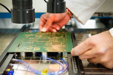
Electrical Testing
Once fabricated, the PCB must be electrically tested to ensure it meets the design specifications and is free of manufacturing defects. There are two main types of testing:
- Bare board testing: Performed on the unpopulated PCB to check for shorts, opens, and continuity between nets. Common tests include:
- Flying probe test: Two probes check each net for continuity and isolation.
- Fixture-based test: The board is placed in a fixture with pins contacting each net, and continuity is checked.
-
Automated optical inspection (AOI): The board is scanned for visual defects.
-
In-circuit testing (ICT): Performed on the populated PCB to check for proper component placement, value, and functionality. This requires a custom test fixture and programming for each board design.
Boards that pass testing are marked and packaged for shipment. Boards that fail are analyzed for the root cause of the failure and reworked or scrapped as necessary.
Cutting and Packaging
The final step in PCB fabrication is cutting the individual boards out of the panel and packaging them for shipment. Cutting is typically done using:
- V-scoring: A V-shaped groove is cut partway through the board along the outline, allowing it to be easily snapped apart.
- Routing: A CNC router cuts completely through the board along the outline.
The boards are then packaged in antistatic bags or boxes with appropriate labeling and documentation, such as the certificate of conformance (CoC) and material data sheets.
PCB Fabrication FAQ
What is the typical lead time for PCB fabrication?
Lead times vary depending on the complexity of the board and the fabrication house, but typical lead times are:
- 1-2 layers: 2-5 days
- 4-6 layers: 3-7 days
- 8+ layers: 5-10 days
Expedited services are often available for an additional cost.
What are the most common PCB sizes?
The most common PCB sizes are:
- 100 x 100 mm
- 150 x 150 mm
- 200 x 200 mm
- 250 x 250 mm
However, PCBs can be fabricated in any size up to the maximum panel size of the fabrication equipment, which is typically 18 x 24 inches (457 x 610 mm).
What are the standard PCB Thicknesses?
The most common PCB thicknesses are:
- 0.8 mm (0.031″)
- 1.6 mm (0.063″)
- 2.4 mm (0.094″)
Thinner and thicker boards are available for specialized applications such as mobile devices and high-power electronics.
What is the minimum feature size for PCB traces?
The minimum feature size depends on the capabilities of the fabrication house, but typical minimums are:
- Trace width: 0.006″ – 0.010″ (0.15 – 0.25 mm)
- Trace spacing: 0.006″ – 0.010″ (0.15 – 0.25 mm)
Smaller features may be possible with specialized processes such as thin film or semi-additive plating.
How much does PCB fabrication cost?
PCB fabrication cost depends on several factors, including:
- Board size
- Number of layers
- Quantity
- Material selection
- Surface finish
- Turnaround time
Typical costs for a medium-complexity board (4-6 layers, 100 x 100 mm) range from $10-$50 per board in quantities of 100 or more. Higher quantities and simpler designs will result in lower per-board costs, while rush orders and specialized materials will increase the cost.
Conclusion
PCB fabrication is a complex process involving many steps and considerations. By understanding the basics of design, materials, manufacturing processes, and testing, you can ensure your PCBs are fabricated to the highest quality standards and meet the requirements of your application. Working closely with your fabrication partner and providing clear and accurate documentation will help streamline the process and minimize delays and errors.


Leave a Reply