Introduction to Solderability Testing
Solderability testing is a crucial process in the manufacturing of printed circuit boards (PCBs) to ensure the quality and reliability of the final product. It involves evaluating the ability of component leads, pins, and PCB pads to be wetted by molten solder during the assembly process. Proper solderability is essential for creating strong, reliable solder joints that can withstand the stresses of normal operation and environmental conditions.
Importance of Solderability Testing
Solderability testing is important for several reasons:
- Quality assurance: It ensures that components and PCBs are suitable for the soldering process, resulting in high-quality solder joints.
- Reliability: Properly soldered joints are critical for the long-term reliability of electronic devices, as poor solderability can lead to weak or failed connections.
- Cost reduction: Identifying solderability issues early in the manufacturing process can help avoid costly rework or product failures in the field.
Factors Affecting Solderability
Several factors can influence the solderability of components and PCBs:
Surface Finish
The surface finish of component leads and PCB pads plays a significant role in solderability. Common surface finishes include:
| Surface Finish | Description | Advantages | Disadvantages |
|---|---|---|---|
| Hot Air Solder Leveling (HASL) | Dipping in molten solder and leveling with hot air | Excellent solderability, low cost | Uneven surface, thermal stress |
| Electroless Nickel Immersion Gold (ENIG) | Nickel plating followed by thin gold layer | Flat surface, good shelf life | Higher cost, black pad issue |
| Immersion Silver (IAg) | Thin silver layer deposited on copper | Lower cost, good solderability | Limited shelf life, tarnishing |
| Immersion Tin (ISn) | Thin tin layer deposited on copper | Lower cost, good solderability | Whisker growth, limited shelf life |
Storage Conditions
Proper storage of components and PCBs is essential for maintaining solderability. Factors to consider include:
- Temperature: High temperatures can accelerate the deterioration of surface finishes.
- Humidity: High humidity can lead to oxidation and tarnishing of surfaces.
- Shelf life: Some surface finishes have limited shelf life and may degrade over time.
Contamination
Contamination of component leads or PCB pads can negatively impact solderability. Common contaminants include:
- Oils and greases from handling
- Flux residues from previous soldering processes
- Oxidation and tarnishing of surfaces

Solderability Testing Methods
There are several methods for evaluating the solderability of components and PCBs:
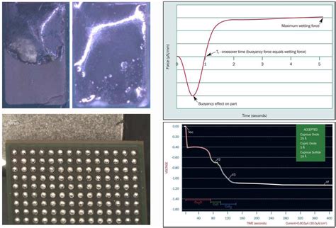
Wetting Balance Test
The wetting balance test measures the wetting force and time of a component lead or PCB pad when dipped into molten solder. The test setup consists of a balance, a solder bath, and a dipping mechanism. The sample is suspended from the balance and dipped into the solder bath at a controlled speed and depth. The wetting force is recorded as a function of time, providing information on the wetting speed and quality.
Dip and Look Test
The dip and look test is a qualitative method for assessing solderability. The component lead or PCB pad is dipped into a solder bath for a specified time and then visually inspected for solder coverage and wetting quality. The results are typically classified into categories such as good, fair, or poor based on the percentage of surface area wetted by the solder.
Solderability Testing Standards
Solderability testing is governed by various industry standards, which provide guidelines for test methods, parameters, and acceptance criteria. Some common standards include:
- IPC-J-STD-002: Solderability Tests for Component Leads, Terminations, Lugs, Terminals, and Wires
- IPC-J-STD-003: Solderability Tests for Printed Boards
- MIL-STD-883: Test Method Standard for Microcircuits
These standards ensure consistency and repeatability in solderability testing across different manufacturers and industries.

Interpreting Solderability Test Results
Interpreting the results of solderability tests is crucial for making informed decisions about component and PCB Quality. Some key factors to consider include:
Wetting Time
The wetting time is the time required for the molten solder to completely wet the surface of the component lead or PCB pad. Shorter wetting times generally indicate better solderability, as the solder can quickly and efficiently form a strong bond with the surface.
Wetting Force
The wetting force is the maximum force exerted by the molten solder on the component lead or PCB pad during the wetting process. Higher wetting forces typically correspond to better solderability, as they indicate a stronger interaction between the solder and the surface.
Visual Inspection
Visual inspection of the solder joint after the solderability test can provide additional information on the quality of the wetting process. A well-soldered joint should exhibit complete and uniform coverage of the surface, with a smooth and shiny appearance. Any signs of dewetting, voids, or contamination may indicate solderability issues.

Improving Solderability
If solderability issues are identified during testing, several steps can be taken to improve the solderability of components and PCBs:
Cleaning
Proper cleaning of component leads and PCB pads can remove contaminants and improve solderability. Cleaning methods may include:
- Solvent cleaning: Using solvents to dissolve and remove oils, greases, and flux residues
- Plasma cleaning: Using a plasma of ionized gas to remove organic contaminants and activate surfaces
- Mechanical cleaning: Using abrasive methods such as brushing or scrubbing to remove surface oxides
Pretinning
Pretinning involves applying a thin layer of solder to the component leads or PCB pads prior to the main soldering process. This can help improve solderability by providing a fresh, oxide-free surface for the molten solder to wet during assembly.
Storage and Handling
Proper storage and handling of components and PCBs can help maintain solderability over time. This includes:
- Storing components and PCBs in a cool, dry environment
- Using moisture barrier bags or desiccants to control humidity
- Minimizing exposure to air and contaminants during handling
Frequently Asked Questions (FAQ)
- Q: What is the purpose of solderability testing?
A: Solderability testing is performed to evaluate the ability of component leads, pins, and PCB pads to be wetted by molten solder during the assembly process. It ensures that the surfaces are suitable for creating strong, reliable solder joints.
- Q: What factors can affect solderability?
A: Several factors can influence solderability, including surface finish, storage conditions, and contamination. The type of surface finish (e.g., HASL, ENIG, IAg) can impact wetting behavior, while improper storage or exposure to contaminants can degrade solderability over time.
- Q: What are the common methods for solderability testing?
A: The two most common methods for solderability testing are the wetting balance test and the dip and look test. The wetting balance test quantitatively measures the wetting force and time, while the dip and look test is a qualitative method that involves visual inspection of solder coverage and wetting quality.
- Q: How can solderability issues be addressed?
A: If solderability issues are identified during testing, they can be addressed through various means, such as cleaning the surfaces to remove contaminants, pretinning the leads or pads to provide a fresh soldering surface, and ensuring proper storage and handling to maintain solderability over time.
- Q: Are there industry standards for solderability testing?
A: Yes, there are several industry standards that govern solderability testing, such as IPC-J-STD-002 for component leads and terminations, IPC-J-STD-003 for printed boards, and MIL-STD-883 for microcircuits. These standards provide guidelines for test methods, parameters, and acceptance criteria to ensure consistency and repeatability in solderability testing.
Conclusion
Solderability testing is a vital process in the manufacturing of electronic devices, as it ensures the quality and reliability of solder joints. By understanding the factors that affect solderability, the various testing methods available, and the interpretation of test results, manufacturers can take proactive steps to improve the solderability of their components and PCBs. This, in turn, leads to higher-quality products, reduced rework and failure rates, and ultimately, greater customer satisfaction.
As the electronics industry continues to evolve, with increasingly complex designs and smaller form factors, the importance of solderability testing will only continue to grow. By staying up-to-date with the latest standards, best practices, and testing technologies, manufacturers can ensure that their products meet the highest standards of quality and reliability, now and in the future.


Leave a Reply