What is a PCB Annular Ring?
A printed circuit board (PCB) annular ring, also known as a pad ring or ring pad, refers to the copper area surrounding a drilled hole on a PCB. The annular ring provides electrical connectivity between the plated through hole (PTH) and the copper trace or plane connected to it. In other words, it acts as a conductive link, allowing electrical current to flow from the component lead inserted into the hole to the rest of the circuit.
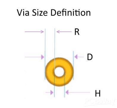
The annular ring consists of two main parts:
- The pad: The flat copper area encircling the drilled hole
- The plating: The conductive coating applied to the walls of the drilled hole, connecting the top and bottom layers of the PCB
Importance of Annular Rings in PCB Design
Annular rings play a crucial role in the functionality, reliability, and manufacturing process of PCBs. Here are some key reasons why annular rings are important:
Electrical Connectivity
The primary purpose of annular rings is to provide electrical connectivity between components and the PCB. Without proper annular rings, the electrical current may not flow effectively, leading to signal integrity issues or even complete circuit failure.
Mechanical Strength
Annular rings also contribute to the mechanical strength of the solder joint between the component lead and the PCB. A larger annular ring provides more surface area for the solder to adhere to, resulting in a stronger and more reliable connection. This is particularly important for components subjected to mechanical stress or vibration.
Manufacturing Consistency
Consistent and well-defined annular rings are essential for the accurate placement and soldering of components during the PCB Assembly process. Proper annular ring design ensures that the holes are drilled accurately and the components are aligned correctly, reducing the risk of manufacturing defects.

Annular Ring Design Considerations
When designing annular rings for your PCB, there are several factors to consider to ensure optimal performance and manufacturability.
Annular Ring Size
The size of the annular ring is a critical design consideration. The annular ring should be large enough to provide sufficient electrical connectivity and mechanical strength but not so large that it compromises the available space for routing traces or placing other components.
The minimum annular ring size is typically determined by the PCB manufacturer’s capabilities and the specific requirements of the design. The following table provides general guidelines for minimum annular ring sizes based on the hole size:
| Hole Size (mm) | Minimum Annular Ring (mm) |
|---|---|
| 0.2 – 0.4 | 0.05 |
| 0.4 – 0.6 | 0.075 |
| 0.6 – 1.0 | 0.1 |
| 1.0 – 2.0 | 0.15 |
| > 2.0 | 0.2 |
It’s important to consult with your PCB manufacturer to determine their specific annular ring requirements and capabilities.
Hole Size and Plating Thickness
The hole size and plating thickness also impact the design of annular rings. The hole size should be appropriate for the component lead diameter, allowing for proper insertion and soldering. The plating thickness should be sufficient to provide reliable electrical connectivity and meet the current carrying requirements of the circuit.
Typical plating thicknesses range from 25 to 50 micrometers (μm) for standard PCBs, but thicker plating may be required for high-current applications or to meet specific industry standards.
Pad Shape and Solder Mask Opening
The shape of the pad and the solder mask opening around the annular ring can affect the soldering process and the final appearance of the solder joint. Common pad shapes include circular, oval, and rectangular, each with its own advantages and disadvantages.
The solder mask opening should be designed to expose the appropriate amount of copper for soldering while providing adequate insulation between adjacent pads. The following table provides general guidelines for solder mask opening sizes based on the pad size:
| Pad Size (mm) | Solder Mask Opening (mm) |
|---|---|
| 0.5 – 1.0 | Pad size + 0.05 |
| 1.0 – 2.0 | Pad size + 0.1 |
| > 2.0 | Pad size + 0.15 |

Annular Ring in Different PCB Types
Annular rings are used in various types of PCBs, each with its own specific requirements and considerations.
Single-Layer PCBs
Single-layer PCBs have copper traces and pads on only one side of the board. The annular rings on single-layer PCBs are relatively simple, as they only need to provide connectivity between the component lead and the copper trace on the same side of the board.
Double-layer PCBs
Double-layer PCBs have copper traces and pads on both sides of the board, with plated through holes connecting the layers. The annular rings on double-layer PCBs must provide connectivity between the component lead and the copper traces on both sides of the board.
Multi-layer PCBs
Multi-layer PCBs consist of three or more conductive layers separated by insulating layers. The annular rings on multi-layer PCBs must provide connectivity between the component lead and the appropriate inner layers, as well as the top and bottom layers. Designing annular rings for multi-layer PCBs requires careful consideration of the layer stack-up and the routing requirements of the circuit.

Annular Ring Defects and Their Impact
Annular ring defects can occur during the PCB manufacturing process and can have a significant impact on the functionality and reliability of the final product. Some common annular ring defects include:
Annular Ring Breakout
Annular ring breakout occurs when the drilling process removes part of the annular ring, reducing its size and potentially compromising the electrical connectivity and mechanical strength of the solder joint. This defect can be caused by misalignment of the drill bit, incorrect drill size, or excessive vibration during drilling.
Insufficient Annular Ring
An insufficient annular ring occurs when the copper area surrounding the hole is too small to provide adequate electrical connectivity or mechanical strength. This defect can be caused by design errors, manufacturing limitations, or excessive etching of the copper during the PCB Fabrication process.
Lifted or Damaged Pads
Lifted or damaged pads can occur when the annular ring is subjected to excessive mechanical stress during the assembly process, such as during component insertion or soldering. This defect can result in poor electrical connectivity or complete separation of the pad from the PCB.
Inspection and Testing of Annular Rings
To ensure the quality and reliability of PCBs, it is essential to inspect and test the annular rings during the manufacturing process and after assembly.
Visual Inspection
Visual inspection is the first line of defense against annular ring defects. This process involves examining the PCB under magnification to check for any visible defects, such as annular ring breakout, insufficient copper, or Lifted Pads.
Automated Optical Inspection (AOI)
AOI is a computer-based system that uses high-resolution cameras and image processing software to inspect PCBs for defects, including annular ring issues. AOI systems can quickly and accurately detect defects that may be missed by visual inspection alone.
Electrical Testing
Electrical testing is performed to verify the continuity and insulation resistance of the PCB, including the annular rings. This testing can be done using various methods, such as flying probe testing, bed-of-nails testing, or in-circuit testing, depending on the complexity of the PCB and the specific requirements of the application.
Best Practices for Annular Ring Design and Manufacturing
To minimize the risk of annular ring defects and ensure the best possible performance and reliability of your PCBs, consider the following best practices:
- Follow the PCB manufacturer’s guidelines for annular ring size, hole size, and plating thickness.
- Use appropriate pad shapes and solder mask openings for your specific application and soldering process.
- Consider the specific requirements of your PCB type (single-layer, double-layer, or multi-layer) when designing annular rings.
- Communicate clearly with your PCB manufacturer regarding your design intent and any special requirements.
- Perform thorough inspection and testing of your PCBs during the manufacturing process and after assembly to identify and correct any annular ring defects.
Frequently Asked Questions (FAQ)
1. What is the difference between an annular ring and a pad?
The annular ring is the copper area surrounding a drilled hole on a PCB, while the pad is the flat part of the annular ring that provides a surface for soldering. The annular ring includes both the pad and the plating inside the hole.
2. Can I use different annular ring sizes for different components on the same PCB?
Yes, you can use different annular ring sizes for different components based on their specific requirements, such as lead diameter, current carrying capacity, and mechanical strength. However, it’s essential to ensure that the annular ring sizes meet the minimum requirements specified by your PCB manufacturer.
3. What happens if the annular ring is too small?
If the annular ring is too small, it may not provide sufficient electrical connectivity or mechanical strength, leading to signal integrity issues, intermittent connections, or even complete failure of the solder joint. In some cases, an insufficient annular ring can also make the PCB more difficult to manufacture and assemble.
4. Can annular ring defects be repaired after PCB assembly?
In some cases, annular ring defects can be repaired after PCB assembly, depending on the severity and location of the defect. For example, lifted pads may be repaired by adding additional solder or using conductive epoxy. However, prevention is always better than cure, and it’s best to catch and correct annular ring defects during the manufacturing process.
5. How can I ensure that my PCB manufacturer follows my annular ring specifications?
To ensure that your PCB manufacturer follows your annular ring specifications, provide clear and detailed design files, including the necessary dimensions, tolerances, and any special requirements. Communicate with your manufacturer throughout the process and request regular updates and inspection reports. If possible, visit the manufacturing facility to discuss your requirements in person and observe the production process.
Conclusion
PCB annular rings are a critical aspect of PCB design and manufacturing, providing the essential electrical and mechanical connection between components and the board. By understanding the importance of annular rings, considering key design factors, and following best practices for manufacturing and inspection, you can ensure the optimal performance, reliability, and manufacturability of your PCBs.
Remember to work closely with your PCB manufacturer, communicate your requirements clearly, and stay informed about the latest industry standards and advancements in PCB technology. With the right knowledge and approach, you can create PCBs with robust and reliable annular rings that meet the demands of your specific application.


Leave a Reply