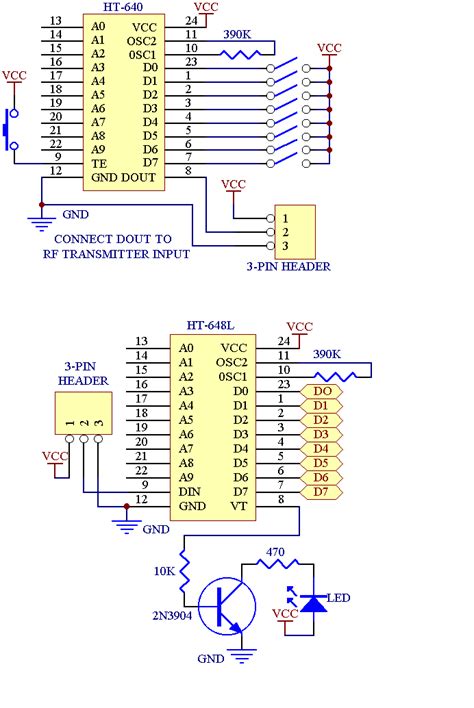
Introduction to the HT12D RF Decoder
The HT12D is a popular radio frequency (RF) decoder integrated circuit (IC) used in many wireless remote control applications. Manufactured by Holtek, this 2^12 series decoder pairs with Holtek’s HT12E RF encoder to form a complete RF transmitter and receiver solution for controlling devices wirelessly.
The HT12D is capable of decoding 12 bits of information, giving it the ability to decode one of 4096 (2^12) unique addresses. This allows for a large number of devices to be controlled independently using the HT12E/HT12D encoder/decoder pair.
Some key features of the HT12D include:
- Operating voltage range of 2.4V to 12V
- Low power and high noise immunity CMOS technology
- Pairs with HT12E 2^12 series of encoders
- Built-in oscillator needs only 5% resistor
- Valid transmission indicator
- Easy interface with an RF or infrared transmission medium
- Minimal external components required
The HT12D is widely used in garage door openers, car door controllers, burglar alarm systems, domestic appliance controllers, and many other remote control applications. Its simplicity, reliability, and low cost make it a popular choice for engineers and hobbyists alike.
How the HT12E/HT12D Encoder/Decoder Pair Works
The HT12E encoder and HT12D decoder ICs work together to transmit and receive 12-bit data in a simple serial format. The 12-bit data consists of 8 address bits and 4 data bits.
Here’s a basic overview of how the HT12E and HT12D work together:
-
The 8 address bits (A0-A7) on the HT12E are set to a unique value by connecting each pin to either Vcc or ground. This creates the address of the remote.
-
The 4 data bits (AD8-AD11) on the HT12E are set based on the state of the buttons or switches on the remote.
-
When a button is pressed on the remote, the HT12E reads the states of the address and data pins and encodes this 12-bit value.
-
The encoded value is transmitted serially through the RF transmitter connected to the HT12E.
-
The RF receiver connected to the HT12D receives the transmitted signal.
-
The HT12D decodes the serial data and checks the received address bits against its locally set address.
-
If the received address matches the local address, the 4 data bits are decoded and output on pins D8-D11 of the HT12D.
-
The valid transmission (VT) pin on the HT12D goes high to indicate a valid data transmission.
This simple yet effective encoding and decoding scheme allows for robust, error-resistant wireless data transmission. The large address space of 256 addresses allows many devices to be controlled independently.

HT12D Pinout and Pin Description
The HT12D is available in 18-pin DIP and 20-pin SOP packages. Here’s a table describing each pin:
| Pin No. | Pin Name | I/O | Description |
|---|---|---|---|
| 1 | OSC1 | I | Oscillator input pin |
| 2 | OSC2 | O | Oscillator output pin |
| 3 | VT | O | Valid transmission, active high |
| 4-11 | A0-A7 | I | Address input pins |
| 12 | GND | – | Ground |
| 13-16 | D11-D8 | O | 4-bit decoded data output |
| 17 | XI | I | Chip enable, active low |
| 18 | Vcc | – | Positive supply |
The image below shows the typical pin connection diagram for the HT12D:
Here’s a brief description of the most important pins:
-
OSC1 and OSC2: These pins are used to connect the external oscillator components. Typically a resistor is connected between these pins to set the oscillator frequency.
-
A0-A7: These are the address input pins. The state of these pins must match the state of the corresponding address pins on the HT12E for the data to be decoded.
-
D8-D11: These are the 4-bit parallel data output pins. The decoded data is output on these pins when a valid transmission is received.
-
VT: This pin goes high when a valid transmission is received, i.e., when the received address matches the local address set by A0-A7.
-
XI: This is the chip enable pin. It is active low, meaning the chip is enabled when this pin is pulled low.

Setting the Address on the HT12D
One of the most important aspects of using the HT12D is setting its address bits. The address bits on the HT12D must match the address bits set on the HT12E for the data to be decoded correctly.
The 8 address bits, A0-A7, are set by connecting each pin to either Vcc (logic 1) or GND (logic 0). This is typically done using jumpers or DIP switches.
For example, if we want to set the address to 10101100, we would connect pins A7, A5, A3, and A2 to Vcc, and pins A6, A4, A1, and A0 to GND.
Here’s a table showing some example address settings:
| Address | A7 | A6 | A5 | A4 | A3 | A2 | A1 | A0 |
|---|---|---|---|---|---|---|---|---|
| 00000000 | GND | GND | GND | GND | GND | GND | GND | GND |
| 01010101 | GND | Vcc | GND | Vcc | GND | Vcc | GND | Vcc |
| 10101010 | Vcc | GND | Vcc | GND | Vcc | GND | Vcc | GND |
| 11111111 | Vcc | Vcc | Vcc | Vcc | Vcc | Vcc | Vcc | Vcc |
It’s important to ensure that the address set on the HT12D exactly matches the address set on the corresponding HT12E. Even a single bit difference will prevent the data from being decoded.

Interfacing the HT12D with an RF Receiver Module
To receive data wirelessly, the HT12D needs to be interfaced with an RF receiver module. The RF receiver demodulates the received RF signal and outputs it as serial data, which is then fed into the HT12D for decoding.
A typical RF receiver module that pairs well with the HT12D is the RXB6 434MHz receiver. This receiver operates at the same frequency as common HT12E transmitters and outputs the demodulated serial data stream.
Here’s how you would typically connect the RXB6 to the HT12D:
- Connect the Vcc pin of the RXB6 to the positive supply (5V).
- Connect the GND pin of the RXB6 to ground.
- Connect the Data pin of the RXB6 to the OSC1 pin of the HT12D.
That’s it! With just these three connections, the HT12D can receive and decode data from an HT12E transmitter.
It’s important to ensure that the RF receiver and transmitter are operating at the same frequency and are using the same encoding scheme (in this case, the HT12 encoding). Mismatched frequencies or encoding will prevent data from being received correctly.
Decoding Data with the HT12D
Once the address is set and the HT12D is properly interfaced with an RF receiver, it’s ready to start decoding data.
The HT12D continuously monitors the input data stream from the RF receiver, looking for a valid transmission. A valid transmission is one where the received address bits match the address bits set on the HT12D’s address pins.
When a valid transmission is received, the HT12D does the following:
-
It raises the VT (Valid Transmission) pin high to indicate a valid transmission.
-
It decodes the 4 data bits and outputs them on pins D8-D11.
-
It keeps the VT pin high and maintains the data on D8-D11 until the transmission ends.
-
When the transmission ends, it pulls the VT pin low and sets D8-D11 to the idle state.
This process repeats for each valid transmission received. The state of the data bits can be read by a microcontroller or used directly to control the state of relays, LEDs, or other output devices.
Here’s a timing diagram showing the relationship between the input data, VT pin, and output data:
              _   _   _   _   _   _   _   _   _
INPUT DATA   | |_| |_| |_| |_| |_| |_| |_| |_| |_
             |<--------- Address --------->|<--- Data --->|
              ___________________________________
  VT PIN                                       |_________
              ___________________________________
OUTPUT DATA                                    |_________
As you can see, the VT pin goes high as soon as a valid address is received and stays high until the transmission ends. The output data bits are only valid when VT is high.
Interfacing the HT12D with a Microcontroller
In many applications, the decoded data from the HT12D needs to be processed by a microcontroller. This allows for more complex control and logic to be implemented.
Interfacing the HT12D with a microcontroller is straightforward. The microcontroller just needs to monitor the state of the VT pin and read the state of the data pins D8-D11 when VT is high.
Here’s a typical connection between the HT12D and a microcontroller:
-
Connect the VT pin of the HT12D to an input pin on the microcontroller. This pin will be used to detect valid transmissions.
-
Connect pins D8-D11 of the HT12D to four input pins on the microcontroller. These pins will be used to read the decoded data bits.
-
Connect the Vcc and GND pins of the HT12D to the power supply and ground of the Microcontroller Circuit.
With these connections in place, the microcontroller can be programmed to respond to the decoded data in any way necessary.
Here’s a simple example of how this might be done in Arduino code:
const int vtPin = 2;    // VT pin connected to digital pin 2
const int d8Pin = 3;    // D8 pin connected to digital pin 3
const int d9Pin = 4;    // D9 pin connected to digital pin 4
const int d10Pin = 5;   // D10 pin connected to digital pin 5
const int d11Pin = 6;   // D11 pin connected to digital pin 6

void setup() {
  pinMode(vtPin, INPUT);
  pinMode(d8Pin, INPUT);
  pinMode(d9Pin, INPUT);
  pinMode(d10Pin, INPUT);
  pinMode(d11Pin, INPUT);
}

void loop() {
  if (digitalRead(vtPin) == HIGH) {  // Check if VT pin is high
    int data = 0;
    data |= digitalRead(d8Pin) << 0;  // Read D8
    data |= digitalRead(d9Pin) << 1;  // Read D9
    data |= digitalRead(d10Pin) << 2; // Read D10
    data |= digitalRead(d11Pin) << 3; // Read D11

    // Do something with the data...

    delay(100); // Wait for transmission to end
  }
}
In this code, the Arduino constantly checks the state of the VT pin. When VT goes high, it reads the state of the four data pins and combines them into a single 4-bit data value. This data can then be used to control the Arduino’s behavior in any way necessary.
Choosing the Right Oscillator Resistor
The HT12D requires an external oscillator to function. This oscillator is used to clock the internal logic of the chip and to synchronize it with the transmitter.
The oscillator frequency is set by a single resistor connected between the OSC1 and OSC2 pins. The value of this resistor determines the oscillator frequency according to the following formula:
f_osc = 1 / (1.1 * R_osc * C_osc)
Where:
– f_osc is the oscillator frequency in Hz
– R_osc is the value of the oscillator resistor in ohms
– C_osc is the internal oscillator capacitance, which is typically 33pF
For most applications, an oscillator frequency of around 150kHz is suitable. This corresponds to an oscillator resistor value of around 51kΩ.
Here’s a table showing some common oscillator resistor values and their corresponding frequencies:
| Resistor Value | Oscillator Frequency |
|---|---|
| 1MΩ | 3kHz |
| 510kΩ | 6kHz |
| 100kΩ | 30kHz |
| 51kΩ | 150kHz |
| 10kΩ | 300kHz |
It’s important to choose an oscillator resistor that matches the value used in the transmitter. If the transmitter and receiver are using different oscillator frequencies, they will be unable to communicate reliably.
HT12D Application Example: Wireless Relay Control
One common application for the HT12E/HT12D pair is wireless relay control. In this application, the state of relays connected to the HT12D is controlled wirelessly by buttons or switches connected to the HT12E.
Here’s a step-by-step guide on how this can be implemented:
- Connect the HT12E to the transmitter circuit:
- Set the address pins (A0-A7) to a unique address.
- Connect the data pins (AD8-AD11) to the buttons or switches.
-
Connect the OSC1 and OSC2 pins to an oscillator resistor.
-
Connect the HT12D to the receiver circuit:
- Set the address pins (A0-A7) to the same address as the HT12E.
- Connect the OSC1 and OSC2 pins to a matching oscillator resistor.
- Connect the VT pin to an LED to indicate valid transmissions.
-
Connect the data pins (D8-D11) to the control pins of the relays.
-
Power on both the transmitter and receiver circuits.
-
When a button is pressed on the transmitter, the corresponding relay on the receiver should switch on or off.
Here’s a schematic showing a typical setup:
          Transmitter                         Receiver

             HT12E                              HT12D
         +-----------+                      +-----------+
    Vcc -|Vcc     AD8|----- Button 1   Vcc -|Vcc      D8|----- Relay 1
         |           |                      |           |
    Osc -|OSC1   AD9 |----- Button 2   Osc -|OSC1     D9|----- Relay 2
         |OSC2   AD10|----- Button 3       |OSC2    D10|----- Relay 3
         |      AD11 |----- Button 4       |        D11|----- Relay 4
         |A0         |                      |A0         |
         |A1         |                      |A1         |
         |A2         |                      |A2         |
         |A3         |                      |A3         |
         |A4         |                      |A4         |
         |A5         |                      |A5     VT  |-----     LED
         |A6         |                      |A6         |
    GND -|GND     A7 |-----------------GND -|GND      A7|-
         +-----------+                      +-----------+
This setup allows for the wireless control of up to four relays using just two ICs and a handful of passive components. The same principles can be extended to control more relays by using multiple HT12D ICs or by using a microcontroller to process the decoded data.


Leave a Reply