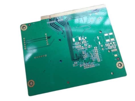
What are PCB Gold Fingers?
PCB Gold Fingers, also known as edge connector contacts or gold-plated contacts, are the gold-plated pads or traces found on the edge of a printed circuit board (PCB). These conductive fingers are designed to establish a reliable electrical connection between the PCB and a mating connector or socket. Gold fingers are commonly found on various types of PCBs, including computer peripherals, memory modules, and expansion cards.
Key Features of PCB Gold Fingers
- Gold plating: The contact pads are plated with a thin layer of gold, which provides excellent conductivity, corrosion resistance, and durability.
- Precise dimensions: Gold fingers are designed to meet specific industry standards, ensuring compatibility with mating connectors.
- Contact area: The gold-plated area is exposed on the edge of the PCB, allowing for easy insertion into a connector or socket.
Why Use Gold for PCB Fingers?
Gold is the preferred material for PCB edge connector contacts due to its unique properties:
- Excellent conductivity: Gold is an exceptional conductor of electricity, ensuring minimal signal loss and reliable connections.
- Corrosion resistance: Gold does not oxidize or tarnish, maintaining its conductivity over time, even in harsh environments.
- Durability: Gold-plated contacts can withstand numerous insertion and removal cycles without significant wear or damage.
- Low contact resistance: Gold provides low contact resistance, which is crucial for high-speed and low-voltage applications.
Comparison of Gold with Other Materials
| Material | Conductivity | Corrosion Resistance | Durability | Contact Resistance |
|---|---|---|---|---|
| Gold | Excellent | Excellent | High | Low |
| Silver | Excellent | Good | Moderate | Low |
| Copper | Good | Poor | Low | Moderate |
| Tin | Moderate | Moderate | Low | High |

PCB Gold Finger Manufacturing Process
The process of creating gold fingers on a PCB involves several steps:
- PCB design: The PCB layout is designed with the appropriate gold finger dimensions and spacing according to industry standards.
- PCB Fabrication: The PCB is manufactured using standard processes, such as etching and drilling.
- Nickel plating: A layer of nickel is plated onto the designated contact areas to provide a barrier between the copper and the gold plating.
- Gold plating: A thin layer of gold, typically between 1 and 3 micrometers, is electroplated onto the nickel surface.
- Surface finish: The gold-plated areas are protected during the solder mask application process, leaving the gold fingers exposed on the edge of the PCB.
Gold Finger Thickness and Specifications
The thickness of the gold plating on PCB fingers is specified in microinches (μin) or micrometers (μm). Common gold plating thicknesses include:
| Thickness (μin) | Thickness (μm) | Application |
|---|---|---|
| 15 – 30 | 0.38 – 0.76 | Low-cost, short-term use |
| 30 – 50 | 0.76 – 1.27 | General-purpose, moderate durability |
| 50 – 100 | 1.27 – 2.54 | High-reliability, long-term use |

PCB Gold Finger Design Considerations
When designing PCBs with gold fingers, several factors must be considered:
- Finger dimensions: The width, length, and spacing of the gold fingers should adhere to industry standards, such as the PCIe or DIMM specifications.
- PCB Thickness: The thickness of the PCB substrate must be compatible with the mating connector.
- Impedance control: For high-speed applications, the impedance of the gold fingers should be controlled to ensure signal integrity.
- Solder mask clearance: The solder mask should be designed to expose the gold-plated areas while protecting the rest of the PCB.
Industry Standards for PCB Gold Fingers
Various industry standards define the dimensions and specifications for PCB gold fingers, depending on the application. Some common standards include:
- PCI Express (PCIe): Defines the connector and gold finger specifications for PCIe expansion cards.
- DIMM (Dual In-line Memory Module): Specifies the gold finger layout and dimensions for memory modules used in computers.
- CompactFlash (CF): Outlines the gold finger design for CompactFlash memory cards.
- Secure Digital (SD): Defines the gold finger layout for SD memory cards.

Testing and Quality Control of PCB Gold Fingers
To ensure the reliability and performance of PCB gold fingers, several testing and quality control methods are employed:
- Visual inspection: Gold fingers are visually inspected for defects, such as scratches, contamination, or uneven plating.
- Thickness measurement: The gold plating thickness is measured using X-ray fluorescence (XRF) or other techniques to ensure compliance with specifications.
- Continuity testing: Electrical continuity between the gold fingers and the PCB circuitry is tested using a multimeter or automated test equipment.
- Insertion and removal testing: The mechanical durability of the gold fingers is evaluated by subjecting them to multiple insertion and removal cycles.
- Environmental testing: PCBs with gold fingers may undergo environmental tests, such as temperature cycling or humidity exposure, to assess their performance under various conditions.
Applications of PCB Gold Fingers
PCB gold fingers are used in a wide range of electronic devices and applications, including:
- Computer peripherals: Expansion cards, such as graphics cards, sound cards, and network adapters, use gold fingers to connect to the motherboard.
- Memory modules: DIMM, SO-DIMM, and other memory modules utilize gold fingers to establish a connection with the memory slots on the motherboard.
- Consumer electronics: Many portable devices, such as smartphones, tablets, and digital cameras, use gold fingers for connecting removable memory cards or other expansion modules.
- Industrial equipment: Gold fingers are used in various industrial applications, such as data acquisition systems, control modules, and communication interfaces.
- Automotive electronics: PCBs with gold fingers are used in automotive electronics, such as infotainment systems, navigation units, and diagnostic tools.
Frequently Asked Questions (FAQ)
-
Q: How long do PCB gold fingers last?
A: The lifespan of PCB gold fingers depends on factors such as the gold plating thickness, the number of insertion and removal cycles, and the operating environment. Typically, gold fingers with a plating thickness of 30 microinches or more can withstand hundreds or even thousands of cycles. -
Q: Can PCB gold fingers be repaired if damaged?
A: In most cases, damaged gold fingers cannot be easily repaired. If the gold plating is worn or scratched, the PCB may need to be replaced. However, minor contamination or oxidation can sometimes be cleaned using specialized products. -
Q: Are there any alternatives to gold for PCB edge connector contacts?
A: While gold is the most common and preferred material for PCB fingers, other materials, such as silver or palladium-nickel alloys, can be used in some applications. However, these alternatives may not provide the same level of conductivity, corrosion resistance, or durability as gold. -
Q: How much does it cost to add gold fingers to a PCB?
A: The cost of adding gold fingers to a PCB depends on factors such as the size of the PCB, the number of fingers, the gold plating thickness, and the manufacturing volume. In general, the cost of gold plating is higher than that of other surface finishes, but it is often justified by the improved performance and reliability. -
Q: Can PCB gold fingers be used for high-frequency applications?
A: Yes, PCB gold fingers are suitable for high-frequency applications, such as high-speed data transmission or RF circuits. However, proper PCB design techniques, such as impedance control and signal integrity management, must be employed to ensure optimal performance.


Leave a Reply