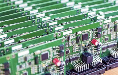
Understanding 10 Layer PCBs
Before diving into the selection process, let’s first understand what a 10 layer PCB is and its advantages.
What is a 10 Layer PCB?
A 10 layer PCB, as the name suggests, consists of ten conductive layers laminated together with insulating material. These layers include:
- Top layer (signal layer)
- Ground layer
- Power layer
- Signal layers (inner layers)
- Bottom layer (signal layer)
The increased number of layers allows for higher routing density, improved signal integrity, and better electromagnetic compatibility (EMC) compared to PCBs with fewer layers.
Advantages of 10 Layer PCBs
- High-density interconnections
- Enhanced signal integrity
- Improved EMC performance
- Reduced board size
- Increased functionality and complexity
Factors to Consider When Choosing a 10 Layer PCB Manufacturer
1. Technical Capabilities
When selecting a 10 layer PCB manufacturer, it’s essential to assess their technical capabilities. Look for manufacturers with experience in producing high-layer count PCBs and a proven track record of delivering quality products.
Consider the following aspects:
- Manufacturing equipment and technology
- Design support and expertise
- Quality control processes
- Certifications (e.g., ISO 9001, UL, RoHS)
2. Material Selection
The choice of materials used in the manufacturing process can significantly impact the performance and reliability of your 10 layer PCB. Discuss material options with potential manufacturers and consider factors such as:
- Dielectric Constant (Dk) and dissipation factor (Df)
- Thermal conductivity
- Copper weight and thickness
- Solder mask and silkscreen options
3. Lead Time and Pricing
Project timelines and budget constraints are critical factors when choosing a 10 layer PCB manufacturer. Inquire about lead times for prototyping and mass production, as well as pricing structures for different quantities.
Keep in mind that while cost is an important consideration, prioritizing quality and reliability is crucial for the success of your project.
4. Communication and Support
Effective communication and support from your PCB manufacturer can make a significant difference in the smooth execution of your project. Look for manufacturers that offer:
- Responsive customer service
- Clear and timely communication
- Technical support and guidance
- Flexibility in accommodating design changes
5. Manufacturing Location
The location of your 10 layer PCB manufacturer can impact factors such as lead time, shipping costs, and communication. Consider the following when evaluating potential manufacturers:
- Proximity to your location
- Shipping options and costs
- Time zone differences for communication
- Language barriers

10 Layer PCB Design Considerations
To ensure the successful manufacturing of your 10 layer PCB, it’s crucial to adhere to best design practices. Consider the following guidelines:
- Use appropriate trace widths and spacing
- Minimize via count and optimize via placement
- Implement proper power and ground plane design
- Follow manufacturer’s design rules and guidelines
- Conduct thorough design reviews and simulations

Frequently Asked Questions (FAQ)
1. What is the typical turnaround time for a 10 layer PCB Prototype?
The turnaround time for a 10 layer PCB prototype can vary depending on the manufacturer and the complexity of your design. Typically, it ranges from 10 to 15 business days, but some manufacturers may offer expedited services for faster delivery.
2. How much does a 10 layer PCB cost compared to a 4 layer PCB?
The cost of a 10 layer PCB is significantly higher than a 4 layer PCB due to the increased complexity and material requirements. The exact price difference depends on factors such as board size, quantity, and manufacturer pricing. On average, a 10 layer PCB can cost 3 to 4 times more than a 4 layer PCB.
3. Can I use a 10 layer PCB for high-frequency applications?
Yes, 10 layer PCBs are well-suited for high-frequency applications due to their improved signal integrity and EMC performance. However, it’s essential to follow best design practices and choose appropriate materials to ensure optimal performance.
4. What are the common materials used in 10 layer PCBs?
Common materials used in 10 layer PCBs include:
| Material | Dielectric Constant (Dk) | Dissipation Factor (Df) | Thermal Conductivity (W/mK) |
|---|---|---|---|
| FR-4 | 4.3 – 4.7 | 0.02 – 0.03 | 0.3 – 0.4 |
| Rogers | 2.5 – 10.2 | 0.0009 – 0.0035 | 0.2 – 1.5 |
| Isola | 3.0 – 4.5 | 0.002 – 0.02 | 0.2 – 0.7 |
5. How can I ensure the manufacturability of my 10 layer PCB design?
To ensure the manufacturability of your 10 layer PCB design:
- Follow the manufacturer’s design guidelines and rules
- Use appropriate trace widths, spacing, and via sizes
- Implement proper power and ground plane design
- Conduct thorough design reviews and simulations
- Communicate with your manufacturer for guidance and feedback

Conclusion
Choosing the right 10 layer PCB manufacturer is a critical decision that can impact the success of your project. By considering factors such as technical capabilities, material selection, lead time, pricing, communication, and manufacturing location, you can make an informed choice that aligns with your project requirements.
Remember to prioritize quality, reliability, and adherence to best design practices to ensure the optimal performance and manufacturability of your 10 layer PCB. By partnering with a reputable and experienced manufacturer, you can bring your complex electronic projects to life with confidence.


Leave a Reply