Ceramic printed circuit boards are made up of several material components layered and integrated together to form a high performance electronic substrate.
The composition and characteristics of the materials strongly influence the properties and capabilities of the ceramic PCB technology.
This article provides an overview of the key components that make up a multilayer ceramic printed circuit board.
Ceramic Substrate
This forms the core foundation layer in a ceramic PCB, providing mechanical support and electrical insulation between conductors.
Some widely used PCB ceramic substrate materials include:
Alumina is the most popular choice, offering the best balance of cost, electrical performance, and mechanical properties.
The substrate is typically 92-96% sintered ceramic with the rest being sintering aids and binders.
Conductor Metallization

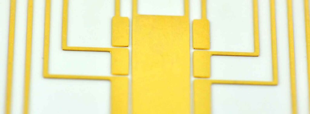
This refers to the conductive circuit traces and features patterned on the ceramic substrate.
Common metallizations used are:
- Gold – Offers excellent conductivity and stability at high temperatures
- Copper – Highly conductive but prone to oxidation at high temperatures
- Silver – Highest conductivity but expensive
- Silver-Palladium – Good conductivity with oxidation resistance
- Tungsten or Moly-Manganese – Refractory metals compatible with co-firing ceramics
Thick film metallization using refractory metals compatible with high co-firing temperatures is typically used. Thin film metallization provides finer features.
Through-Hole Vias
These are plated holes that provide electrical connections between the conductor layers vertically interconnecting tracks on different layers.
High temperature compatible metallizations like tungsten or moly-manganese are used to fill the vias and connect between layers.
Dielectric Layers
These are insulating ceramic layers separating the patterned conductor layers, providing electrical isolation between layers.
The dielectric layers typically use the same base ceramic material as the core substrate for co-firing compatibility.
In embedded passive designs, dielectric layers may incorporate passive components like resistors and capacitors.
Pad and Edge Metallization
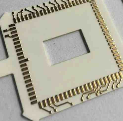
This refers to metallization on exposed pads/lands for component soldering and plating on board edges to facilitate connections.
Nickel-gold plating provides solderability and contact stability. Noble metals like gold or palladium are chosen for stability at high temperatures.
Plated Through Holes
Holes drilled through the entire PCB thickness are activated and plated to interconnect between layers and board edges.
Electroless plating provides conductive continuity before final electrolytic plating with nickel-gold for wear resistance and solderability.
Solder Mask Layer
A solder mask layer is often applied over the outer conductor layers leaving pads exposed for soldering components.
Thick polymer or glass based solder mask materials stable at high temperatures are used.
Legend Print
Identifying labels and markings are printed using thick film inks or thin film metallization to designate components, connections and circuits.
Components
Discrete SMD components, connectors, integrated circuits and modules are soldered onto the pads/lands on the outer surfaces to form the functional electronic circuitry.
High temperature solders and adhesives provide stable attachment. Some components are also directly bonded to pads.
FAQs

What are ceramic PCBs used for?
Ceramic PCBs are typically used for specialized applications with demanding temperature, power, frequency, shock, vibration or other extreme requirements like in aerospace, military, automotive and oil drilling industries.
How are components attached to ceramic PCBs?
Soldering with high-temperature alloys, conductive epoxy adhesives and direct copper bonding are common methods to attach components onto ceramic PCB surfaces and pads.
What metal is used in ceramic PCBs?
Refractory metals like tungsten or moly-manganese allow co-firing with the ceramic at high temperatures. Copper and silver provide the best conductivity but require lower temperature processing.
Can you solder to ceramic PCBs?
Yes, active brazing alloys are specially formulated to wet and solder to ceramics. Plated edge and pad metallization helps improve solderability.
Are vias plated in ceramic PCBs?
Yes, through-hole vias in ceramic PCBs are plated, typically with electroless copper and electrolytic nickel-gold, to provide vertical layer-to-layer and board edge interconnects.
In summary, the specialized material components used in ceramic PCBs enable their exceptional performance meeting challenging application requirements unachievable using standard FR4 PCBs.


Leave a Reply