Understanding PCB Opens and Their Impact on Circuit Functionality
Printed Circuit Boards (PCBs) are essential components in modern electronics, acting as the backbone for interconnecting various electronic components. However, during the manufacturing process or due to external factors, issues like PCB opens can arise, compromising the functionality and reliability of the circuit. In this comprehensive article, we will delve into the concept of PCB opens, their causes, detection methods, and preventive measures.
What is a PCB Open?
A PCB open, also known as an “open circuit,” refers to a situation where there is an unintended break or discontinuity in the conductive paths (traces or vias) on a printed circuit board. This discontinuity prevents the electrical current from flowing through the intended path, leading to a malfunction or complete failure of the connected components or the entire circuit.
Causes of PCB Opens
Several factors can contribute to the occurrence of PCB opens during manufacturing or post-production stages:
- Manufacturing Defects:
- Incomplete etching of the copper traces
- Improper drilling or plating of vias
- Contamination or debris on the PCB surface
-
Incorrect alignment of layers during the lamination process
-
Mechanical Stress:
- Bending or flexing of the PCB
- Impact or shock during handling or transportation
-
Thermal stress due to extreme temperature changes
-
Environmental Factors:
- Corrosion due to exposure to moisture or harsh chemicals
- Electrostatic discharge (ESD) events
-
Vibrations or mechanical shocks during operation
-
Design Issues:
- Insufficient trace width or thickness
- Improper spacing between traces or components
- Incorrect component placement or orientation
Impact of PCB Opens on Circuit Functionality
PCB opens can have severe consequences on the functionality and reliability of electronic circuits:
- Signal Interruption:
- Opens in signal traces disrupt the flow of information between components
-
Incorrect or missing signals can lead to erratic behavior or complete failure
-
Power Supply Issues:
- Opens in power supply traces can prevent components from receiving the necessary power
-
Inadequate power supply can cause components to malfunction or not operate at all
-
Intermittent Faults:
- Intermittent opens can cause sporadic failures that are difficult to diagnose
-
These faults may occur only under specific conditions, making troubleshooting challenging
-
Reduced Reliability:
- PCB opens can compromise the overall reliability of the circuit
- Unaddressed opens can lead to premature failure or reduced lifespan of the product
Detecting PCB Opens
Identifying PCB opens is crucial for ensuring the proper functioning of the circuit. Several methods can be employed to detect opens:
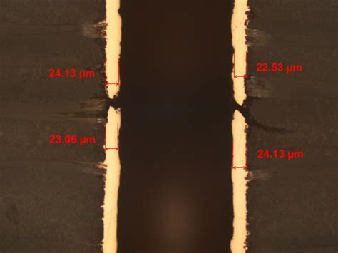
Visual Inspection
A visual inspection is the first step in identifying PCB opens. This involves examining the PCB surface under magnification to look for visible breaks, cracks, or discontinuities in the traces or vias. However, visual inspection may not be sufficient to detect all opens, especially those that are hidden or occur intermittently.
Continuity Testing
Continuity testing involves using a multimeter or a dedicated Continuity Tester to check the electrical continuity between two points on the PCB. By placing the probes on the respective pads or test points, the presence of an open can be confirmed if there is no continuity or if the resistance is significantly higher than expected.
| Test Points | Expected Continuity | Actual Continuity |
|---|---|---|
| TP1 – TP2 | Yes | No |
| TP3 – TP4 | Yes | Yes |
| TP5 – TP6 | Yes | No |
In-Circuit Testing (ICT)
In-Circuit Testing (ICT) is an automated testing method that utilizes a bed-of-nails fixture to make contact with specific test points on the PCB. The ICT system applies electrical stimuli and measures the response to verify the continuity and functionality of the circuit. ICT can detect opens by comparing the measured values against predefined thresholds.
Flying Probe Testing
Flying probe testing is another automated testing technique that uses movable probes to make contact with the desired test points on the PCB. The probes can be programmed to move across the board and perform continuity checks at various locations. Flying probe testing is particularly useful for detecting opens in hard-to-reach areas or on boards with high component density.
X-Ray Inspection
X-ray inspection is a non-destructive testing method that allows the visualization of the internal structure of the PCB. By capturing X-ray images of the board, opens in Buried Vias, inner layers, or hidden traces can be detected. X-ray inspection is especially valuable for identifying opens in Multi-layer PCBs or in areas obscured by components.

Preventing PCB Opens
Preventing PCB opens is crucial to ensure the reliability and longevity of electronic products. Several strategies can be employed to minimize the occurrence of opens:
Robust PCB Design
A well-designed PCB layout is the first line of defense against opens. Consider the following design guidelines:
- Use appropriate trace widths and thicknesses based on the current requirements
- Maintain sufficient spacing between traces and components to avoid short circuits
- Incorporate strain relief features to minimize mechanical stress on the board
- Adhere to the manufacturer’s design rules and guidelines
Quality Control during Manufacturing
Implementing strict quality control measures during the PCB manufacturing process can help prevent opens:
- Conduct thorough inspections at various stages of production
- Use automated optical inspection (AOI) systems to detect defects
- Perform electrical testing to verify continuity and functionality
- Maintain a clean and controlled manufacturing environment
Proper Handling and Storage
Proper handling and storage practices can minimize the risk of PCB opens:
- Use ESD-safe packaging and handling procedures to prevent electrostatic discharge damage
- Store PCBs in a cool, dry environment to avoid moisture-related issues
- Implement proper handling techniques to minimize mechanical stress during assembly and transportation
Environmental Protection
Protecting PCBs from harsh environmental conditions can help prevent opens caused by corrosion or contamination:
- Apply Conformal Coating to shield the PCB from moisture and chemicals
- Use sealed enclosures or potting compounds to protect the board from vibrations and shocks
- Incorporate humidity control measures in the operating environment

Frequently Asked Questions (FAQ)
-
Q: What is the difference between a PCB open and a short circuit?
A: A PCB open refers to a break or discontinuity in the conductive path, preventing current flow. In contrast, a short circuit occurs when two separate conductive paths are unintentionally connected, allowing current to flow through an unintended route. -
Q: Can PCB opens be repaired?
A: In some cases, PCB opens can be repaired using techniques such as jumper wires, conductive ink, or micro-soldering. However, the feasibility of repair depends on factors like the location and extent of the open, the PCB’s complexity, and the available repair equipment and expertise. -
Q: How can PCB opens affect the performance of a circuit?
A: PCB opens can disrupt signal integrity, cause power supply issues, and lead to intermittent or complete failure of the circuit. They can result in erratic behavior, reduced functionality, or total non-operation of the affected components or the entire system. -
Q: What are the most common causes of PCB opens during manufacturing?
A: Common causes of PCB opens during manufacturing include incomplete etching, improper drilling or plating, contamination, and incorrect alignment of layers. These defects can arise due to process variations, equipment malfunctions, or human errors. -
Q: How can X-ray inspection help in detecting PCB opens?
A: X-ray inspection allows non-destructive visualization of the internal structure of a PCB. It can reveal opens in buried vias, inner layers, or traces that are hidden or obscured by components. X-ray inspection is particularly useful for detecting opens in multi-layer PCBs or in areas that are difficult to access with other testing methods.

Conclusion
PCB opens are a critical issue that can significantly impact the functionality, reliability, and lifespan of electronic products. Understanding the causes, detection methods, and preventive measures for PCB opens is essential for manufacturers, designers, and quality assurance professionals.
By implementing robust PCB design practices, strict quality control measures, proper handling and storage techniques, and environmental protection strategies, the occurrence of PCB opens can be minimized. Early detection and timely repair of opens are crucial to ensure the proper functioning of the circuit and avoid costly failures or product returns.
As technology advances and PCBs become more complex, the importance of addressing PCB opens will only increase. By staying informed about the latest techniques and best practices for preventing and detecting opens, manufacturers can deliver high-quality, reliable electronic products to their customers.


Leave a Reply