First article inspection (FAI) for a ceramic PCB is a documented, one-time verification that the manufacturing process produces boards matching every requirement on the drawing and purchase order. Understanding first article inspection PCB procedures is critical because ceramic substrates introduce process variability—fired shrinkage, metallisation adhesion, camber—that organic boards do not. The FAI happens on the first production-representative unit (or a small sample) before the rest of the lot proceeds. If it fails, production stops until the root cause is resolved. If it passes, the report becomes the quality baseline for every subsequent lot.
Key Takeaways
- First article inspection PCB requirements are governed by AS9102 (aerospace) or customer-specific procedures; they are not optional for Class 3 or mission-critical ceramic boards.
- A ceramic FAI typically covers 15–30 measurable characteristics: dimensions, metallisation thickness, dielectric strength, surface finish composition, and substrate flatness.
- Ceramic substrates introduce inspection points that FR-4 boards do not, including fired-shrinkage tolerance, via fill density, and post-fire camber.
- A complete FAI package contains three AS9102 forms: Part Number Accountability (Form 1), Product Accountability (Form 2), and Characteristic Accountability (Form 3).
What Is First Article Inspection for a PCB?
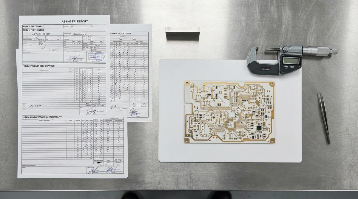
FAI is a formal quality method defined in AS9102 (Rev B, current as of 2024) by SAE International. It requires the manufacturer to measure every characteristic called out on the engineering drawing, compare each measurement to the tolerance, and record the result in a structured report. The purpose is to prove that tooling, fixturing, process parameters, and raw materials together produce a conforming part.
FAI is triggered by any of these events: a new part number entering production, a change in manufacturing process or location, a lapse of more than two years since the last production run, or a change in sub-tier supplier for a critical material such as the ceramic substrate blank. In ceramic PCB work, a switch from one alumina supplier to another—even at the same purity grade—constitutes a process change and should trigger a new FAI.
Why Ceramic PCBs Need Stricter First Article Inspection PCB Procedures
FR-4 fabrication tolerances are well characterised across hundreds of shops. Ceramic substrates behave differently. Fired alumina and aluminium nitride shrink 15–20 % during sintering, and the final dimensional accuracy depends on the green-tape lot, furnace profile, and moisture content at the time of pressing. A via that measures 0.20 mm on the green sheet may finish at 0.16–0.17 mm after firing. These variables make first article inspection PCB dimensional verification essential.
Metallisation adhesion is another ceramic-specific concern. Thick-film silver or gold conductors are screen-printed and fired at 850 °C. Thin-film sputtered layers depend on surface roughness and vacuum conditions. Neither process has the self-correcting etch chemistry of copper-clad laminate. A first article confirms that peel strength (per ASTM F1842 or IPC-TM-650, method 2.4.21) meets the minimum before hundreds of boards go through the furnace.
Post-fire camber and flatness control also matters. Ceramic substrates are brittle; a board that exceeds the camber limit may crack during die attach or reflow. The FAI report should record bow and twist per IPC-TM-650 method 2.4.22.
What Gets Measured During a First Article Inspection PCB Review
The exact list depends on the drawing, but the table below covers the characteristics most commonly inspected on ceramic circuit boards.
| Characteristic | Method / Equipment | Typical Tolerance | Governing Standard |
|---|---|---|---|
| Overall length & width | CMM or optical comparator | ±0.05–0.10 mm | Drawing callout |
| Substrate thickness | Micrometer | ±0.025 mm (for 0.635 mm nominal) | Drawing callout |
| Via diameter | Optical microscope / X-ray inspection for internal vias | ±0.02 mm | Drawing callout |
| Trace width & spacing | AOI or optical measurement | ±0.01–0.025 mm (DPC); ±0.05 mm (thick film) | IPC-6012, Class 3 |
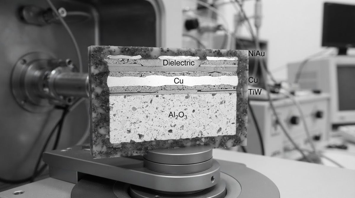
| Metallisation thickness | XRF or cross-section SEM | Per spec (e.g., 5–15 µm Ag thick film) | Drawing callout |
| Surface finish composition | XRF | Per IPC-4552/4553/4556 | IPC-4552 (ENIG) or applicable |
| Dielectric strength | Hipot tester | ≥ 15 kV/mm (96 % Al₂O₃) | IEC 60672-3 |
| Bow & twist (camber) | Surface profilometer or glass plate + feeler gauge | ≤ 0.1 % of diagonal | IPC-TM-650, 2.4.22 |
| Adhesion / peel strength | Pull tester | ≥ 8 N/mm (thick film on Al₂O₃) | ASTM F1842 |
| Visual / cosmetic | 10× magnification inspection | No cracks, chips > 0.1 mm, delamination | IPC-A-600, Class 3 |
Typical values for commercially available material, for comparison only. Confirm against the datasheet for your specific grade.
Environmental screening—such as thermal shock testing—is sometimes included in the FAI package, especially for aerospace or automotive programs. A common requirement is 100 cycles from −55 °C to +125 °C per MIL-STD-883, method 1010, with visual and electrical re-test afterward.
Enter your substrate material, thickness, and operating temperature range below to see which inspection characteristics are most critical for your design and where derating limits apply.
The Three AS9102 Forms
Form 1 – Part Number Accountability. Lists the top-level part number, revision, drawing number, and every sub-component or raw material lot used. For a ceramic PCB, this includes the substrate blank lot number, paste or target lot, and surface finish chemistry lot.
Form 2 – Product Accountability. Traces raw materials and sub-tier sources. This is where ceramic lot traceability and serialisation feeds directly into the FAI. Each substrate blank should carry a lot code traceable to the powder batch and sintering run.
Form 3 – Characteristic Accountability. The core of the report. Every balloon number on the drawing gets a row: nominal value, tolerance, actual measured value, and pass/fail. If any characteristic fails, the form records the nonconformance number and disposition.
Worked Example: Reading a Form 3 Entry
Suppose the drawing calls out substrate thickness at 0.635 mm ± 0.025 mm. The inspector measures the first article at 0.648 mm.
- Nominal: 0.635 mm. Upper limit: 0.660 mm. Lower limit: 0.610 mm.
- Measured value: 0.648 mm. This falls within the tolerance band.
- Result: Pass. The cell is marked with a “C” (conforming) in AS9102 convention.
If the measurement had been 0.665 mm, the entry would be marked “NC” (nonconforming). Production would hold until engineering dispositions the deviation—accept-as-is, rework, or scrap.
When First Article Inspection Is Not Enough
FAI proves the process can make a good part. It does not prove every part in the lot is good. Ongoing in-process inspection—automated optical inspection for trace defects, hipot testing at 100 % for dielectric integrity, and sample-based cross-sectioning—remains necessary throughout production. Think of FAI as the gate; lot acceptance testing is the fence.
When You Do Not Need a Formal First Article Inspection PCB Report
If you are building a prototype run of 5–10 boards for bench validation, a full AS9102 package adds cost and lead time with limited return. A dimensional check report and a material certificate of conformance (C of C) are usually sufficient at this stage. Save the formal FAI for the first production lot or when your end-customer’s quality clause mandates it. Similarly, commercial-grade boards destined for non-safety consumer electronics rarely justify the overhead of a three-form FAI.
If your board is standard FR-4 at IPC Class 2 tolerances, most fabricators handle inspection internally without a customer-facing FAI report. The formal first article inspection PCB process pays for itself on ceramic substrates precisely because the material and process variability is higher.
FAQ
How many boards are inspected during a ceramic PCB FAI?
Typically one to three boards from the first production-representative run. AS9102 requires at least one. Some customers specify three for destructive tests (cross-section, peel strength) so that one intact board remains for the file.
Does a new surface finish trigger a new FAI?
Yes. Changing from ENIG to ENEPIG, or from bare gold thick film to electroplated nickel-gold, alters solderable surface composition and thickness. Both are inspected characteristics, so a delta or full FAI is required.
Can I reuse a previous FAI if only the panel layout changed?
No. A change in panelisation affects shrinkage uniformity, registration, and scoring or laser-scribed break-out dimensions. AS9102 treats any tooling change as a trigger for re-inspection.
How long does a ceramic PCB FAI report stay valid?
AS9102 does not set an expiration date, but most aerospace primes require a new FAI if more than 24 months pass without production. Some automotive OEMs set 12 months. Check your customer’s quality clause.
What is the difference between FAI and PPAP?
PPAP (Production Part Approval Process) is the automotive equivalent, governed by AIAG. It includes the same dimensional data but adds process capability studies (Cpk), control plans, and FMEA. Aerospace programs use AS9102 FAI. The data overlap is roughly 70 %, but the forms and submission rules differ.
Who signs off on the FAI—supplier or customer?
The supplier’s quality engineer completes and signs the forms. The customer’s quality representative reviews and approves. Both signatures are required before the lot ships on most Class 3 and aerospace contracts.
Next Step
If you are preparing for a first article inspection PCB run on a ceramic board, gather your latest-revision Gerber files, drawing with GD&T callouts, and any customer quality clauses. A clear drawing with ballooned characteristics speeds the FAI process by days. When you are ready, request a quote and specify “FAI required” so the inspection scope is included in the lead time estimate.