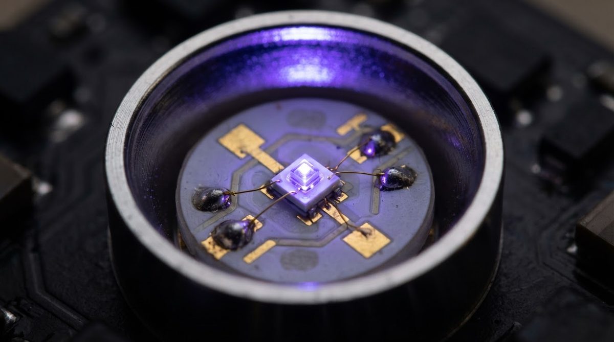
A UVC LED starboard is a metallized aluminum nitride (AlN) substrate—typically 10–25 mm across—designed to mount one or more UV-C LED die or packages and conduct their waste heat into a heatsink. AlN is the standard choice for a UVC LED starboard because its thermal conductivity of 170–200 W/mK (per Kyocera and Maruwa datasheets, at 20 °C) keeps junction temperatures low enough to preserve the notoriously short lifetimes of UV-C emitters operating at 260–280 nm.
Why a UVC LED Starboard Needs AlN Ceramic
UV-C LEDs convert only 3–10 % of input electrical power into UV photons (Nichia NCSU334B datasheet, 2023). The remaining 90–97 % becomes heat concentrated in a die area of roughly 1 × 1 mm. At a typical drive current of 350 mA and forward voltage of 6 V, a single die dissipates about 1.9 W thermally. Junction temperature directly governs both radiant flux and lifetime: every 10 °C rise above 25 °C can reduce L70 lifetime by 20–30 %, according to Seoul Viosys application notes.
A standard FR-4 PCB has a thermal conductivity of only 0.25–0.35 W/mK. Even a metal-core PCB (MCPCB) with an aluminum base reaches about 1–4 W/mK through its dielectric layer. Neither can spread heat fast enough to keep a UV-C die below its rated 85 °C junction limit at useful drive currents. AlN, at 170–200 W/mK, reduces the thermal resistance from die to heatsink by roughly two orders of magnitude compared to FR-4, making it the practical minimum for UVC LED starboard packaging.
AlN Properties That Matter for UVC LED Starboard Design
| Parameter | AlN (typical) | Unit | Condition | Source |
|---|---|---|---|---|
| Thermal conductivity | 170–200 | W/mK | 20 °C | Kyocera SH-170 / Maruwa AN-200 |
| CTE | 4.4–4.7 | ppm/°C | 20–400 °C | CoorsTek ADS-995 |
| Dielectric strength | 15–17 | kV/mm | 25 °C, ASTM D149 | Kyocera SH-170 |
| Flexural strength | 300–400 | MPa | ASTM C1161 | Maruwa AN-200 |
| UV-C reflectance (uncoated) | ~70–80 | % | 265 nm, polished surface | Tokuyama AN datasheet |
| Volume resistivity | >10¹⁴ | Ω·cm | 25 °C | CoorsTek ADS-995 |
Typical values for commercially available material, for comparison only. Confirm against the datasheet for your specific grade.
Two properties stand out beyond raw thermal conductivity. First, AlN’s CTE of 4.4–4.7 ppm/°C closely matches the sapphire or AlN sub-mounts used inside UV-C LED packages (CTE 4.5–7.1 ppm/°C for sapphire). This reduces solder-joint stress during thermal cycling. Second, uncoated AlN reflects 70–80 % of 265 nm light, which helps redirect stray photons into the target zone rather than absorbing them as additional heat. Al₂O₃, by contrast, absorbs more strongly in the deep UV.
Starboard Layout and Metallization Options
A typical UVC LED starboard carries one to four LED packages on a square or circular AlN substrate, 0.25–1.0 mm thick. The metallization pattern provides solder pads for the LED anode and cathode, a large thermal pad beneath the LED, and sometimes a reflective border area.
Metallization options
DPC (Direct Plated Copper) is the most common process for UVC LED starboard production. A sputtered Ti/Cu seed layer followed by electrolytic copper plating produces traces 20–100 µm thick with fine feature resolution. DPC on AlN is well-suited to the small geometries and tight pad pitches of UV-C LED packages. You can learn more about this process on our page covering AlN DPC ceramic substrates.
Thin-film metallization (sputtered Ti/Pt/Au or Ti/Ni/Au) is used when pad pitch drops below 100 µm or when gold wire bonding directly to the substrate is required. This is more expensive per unit but eliminates solder voids under the die.
Thick-film (screen-printed Ag or Au) is viable for larger LED packages with relaxed tolerances. It is the lowest cost per board but limited to roughly 100 µm minimum line/space.
Surface finish
ENIG or ENEPIG finishes are standard for SMD reflow soldering of UV-C LED packages. For die-attach applications using AuSn solder preforms, an electroplated Au finish (2–5 µm) over a Ni barrier is preferred to ensure wettability and minimize voiding.
Worked Example: Thermal Resistance of a Single-LED Starboard
Consider a single UV-C LED (1.9 W thermal dissipation) mounted on a 15 × 15 mm AlN starboard, 0.38 mm thick, with a 3 × 3 mm thermal pad.
Step 1 — Substrate conduction. Thermal resistance through the AlN: Rth = t / (k × A) = 0.00038 m / (180 W/mK × 9 × 10⁻⁶ m²) = 0.23 °C/W. Here k = 180 W/mK (mid-range AlN) and A = 3 × 3 mm pad area.
Step 2 — Spreading resistance. Heat spreads laterally through the full 15 × 15 mm substrate. Using the analytical spreading-resistance approximation (Song, Lee & Au, 1994), the additional spreading resistance is roughly 0.6–0.9 °C/W depending on heatsink interface.
Step 3 — Total die-to-heatsink. Adding solder-joint resistance (~0.1 °C/W for a well-soldered pad) and thermal interface material (~0.3 °C/W), the total Rth from LED junction to heatsink is approximately 1.2–1.5 °C/W. At 1.9 W dissipation, the temperature rise above heatsink is about 2.3–2.9 °C. That keeps junction temperature well within limits, even with a heatsink at 60 °C.
Compare this to an MCPCB with a 2 W/mK dielectric layer, 75 µm thick, same pad area: Rth(dielectric) = 0.000075 / (2 × 9 × 10⁻⁶) = 4.2 °C/W through the dielectric alone—roughly 18× higher than the AlN substrate path.
Enter your substrate dimensions, thickness, and LED power dissipation below to estimate junction temperature rise for your own UVC LED starboard design.
Starboard Shape and Sourcing Checklist
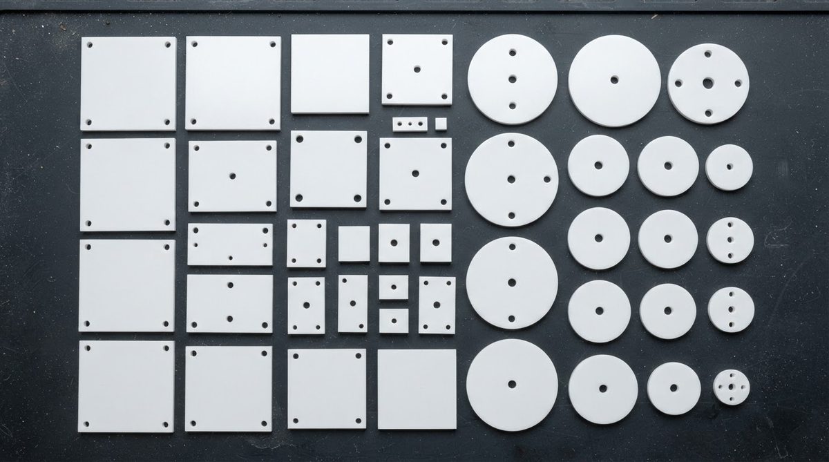
UV-C starboards are typically supplied as individual substrates, laser-scribed or laser-cut AlN parts from a larger panel. Common shapes are square (10 × 10, 15 × 15, 20 × 20 mm) and circular (Ø 16, Ø 20 mm). Circular starboards fit directly into reflector cup assemblies used in point-source disinfection modules.
When ordering a UVC LED starboard, specify the following:
- Substrate grade: 170 W/mK or 200 W/mK AlN
- Thickness: typically 0.25, 0.38, 0.50, or 1.0 mm
- Metallization type: DPC, thin-film, or thick-film
- Surface finish: ENIG, ENEPIG, or electroplated Au
- Delivery format: bare aluminum nitride blanks or fully metallized and patterned boards
When Not to Use an AlN Starboard
UV-A or visible-light LEDs. LEDs emitting above 350 nm have wall-plug efficiencies of 30–60 %, generating far less heat per watt of optical output. An MCPCB or even FR-4 with thermal vias is often sufficient and much cheaper.
Very low drive currents. If you are running a UV-C LED at ≤50 mA for sensing rather than disinfection, total dissipation may be under 0.2 W. A 96 % alumina substrate (24–28 W/mK) handles this at a fraction of AlN’s cost. See our guide to ceramic PCB materials for a full comparison.
Large arrays where cost dominates. For panels carrying dozens of UV-C LEDs at moderate currents, a hybrid approach—AlN sub-mounts soldered to an aluminum MCPCB—can balance thermal performance and cost. The sub-mount handles the immediate die-level heat spreading; the MCPCB handles bulk heat transport to the chassis.
Flexible or non-planar geometries. AlN is a rigid ceramic. If your design requires a curved emitter surface, consider a flexible MCPCB with individual AlN thermal pads bonded at each LED site.
Frequently Asked Questions
Does UV-C light degrade the AlN substrate over time?
AlN is chemically stable under UV-C irradiation at 260–280 nm. Unlike organic PCB materials, it does not yellow, crack, or outgas under prolonged UV exposure. The metallization and solder joints are the lifespan-limiting factors, not the ceramic.
Can I use Al₂O₃ instead of AlN for a UVC LED starboard?
You can, but only at low power levels. 96 % alumina’s thermal conductivity (24–28 W/mK) is roughly 7× lower than AlN. For a single LED driven above 200 mA, junction temperatures will rise significantly. Alumina also absorbs more UV-C energy than AlN, reducing optical efficiency of the module.
What solder is best for attaching UV-C LEDs to an AlN starboard?
SAC305 (Sn96.5/Ag3.0/Cu0.5) is standard for SMD UV-C packages reflowed at 245–260 °C peak. For bare-die attach requiring higher reliability, AuSn (80/20) solder preforms reflowed at 310–320 °C are common. Indium-based solders are sometimes used for lower-stress bonding but have lower thermal conductivity.
What is the typical lead time for custom UVC LED starboards?
Prototype quantities of metallized AlN starboards typically ship in 2–4 weeks depending on metallization process and surface finish. Production volumes may require 4–8 weeks. Confirm with your supplier early, especially for thin-film metallization which has longer processing cycles.
Do I need a conformal coating on the starboard?
Generally no. Most organic conformal coatings degrade rapidly under UV-C exposure. If moisture protection is needed, use a hermetic housing or an inorganic passivation layer (e.g., SiO₂ sputtered film) on exposed traces. The AlN ceramic itself is inherently moisture-resistant.
Next Step
If you are specifying a UVC LED starboard, start by defining your LED package footprint, thermal dissipation, and required substrate dimensions. For a full walkthrough of ceramic substrate capabilities, visit our ceramic PCB FAQ. Ready to get pricing on AlN starboards? Request a quote directly.