Screen printing ceramic capability tops out at fired conductor line widths down to 100 µm, line spacing down to 100 µm, and per-pass thicknesses of 10–50 µm depending on mesh count and paste rheology. It is the dominant deposition method for thick-film circuits on Al₂O₃ and AlN, offering a practical balance of cost, throughput, and resolution that sits between sputtered thin-film metallization and direct bonded copper. Understanding screen printing ceramic capability in detail lets you set accurate design rules and avoid over-specifying a costlier process.
Key Takeaways
- Minimum printed line width is 100–150 µm with a 325-mesh stainless-steel screen; finer features require thin-film processes.
- Fired thickness per pass ranges from roughly 10 µm (fine mesh, low-viscosity paste) to 50 µm (coarse mesh, high-solids paste), per typical DuPont and Heraeus thick-film datasheet values.
- Registration accuracy of ±25–50 µm is standard; tighter alignment demands fiducial-based vision systems.
- Conductor, resistor, and dielectric pastes can be printed sequentially on the same substrate, enabling embedded passives without added components.
- Screen printing is not suited for features below about 75 µm or for copper layers thicker than roughly 50 µm per pass. For heavier copper, see heavy copper capabilities on ceramic.
What Is Screen Printing on Ceramic?
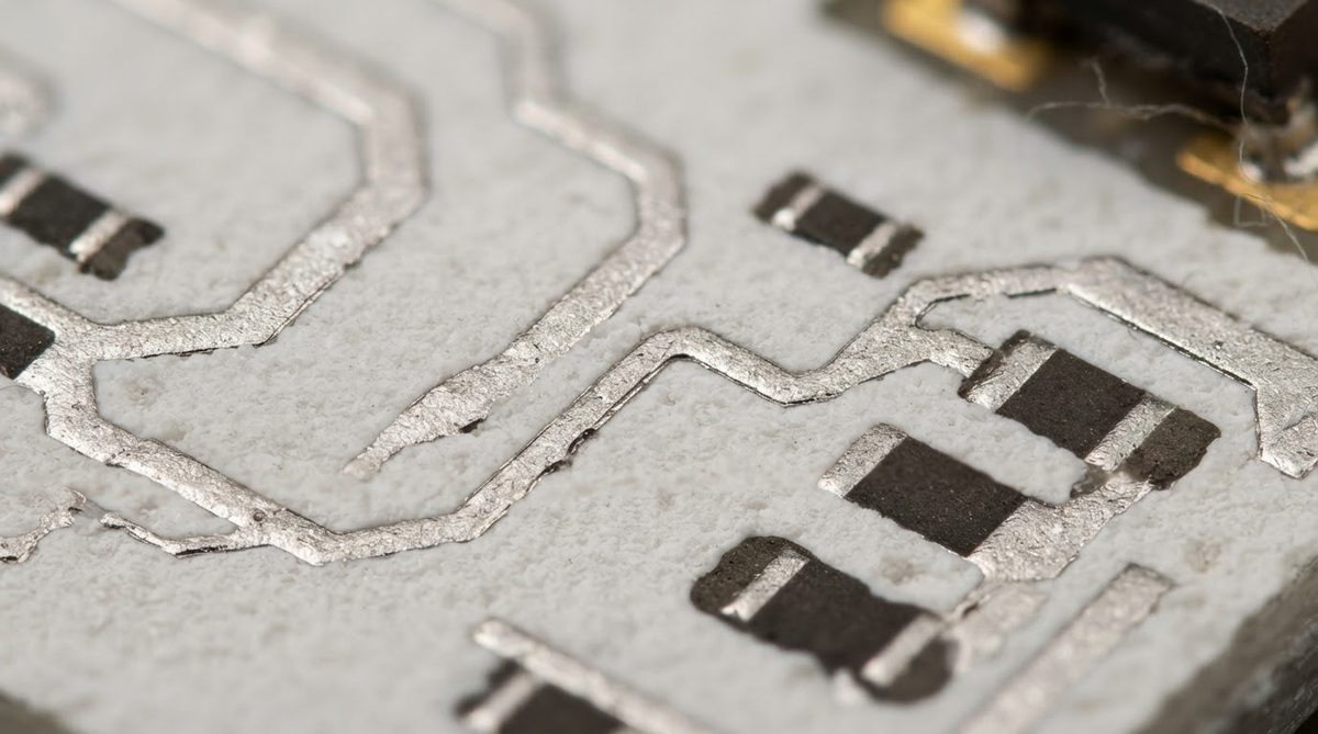
Screen printing is an additive deposition process. A patterned stainless-steel or polyester mesh screen is stretched over a frame. Paste—containing metal particles (Ag, Au, Pt, Pd, or Cu), glass frit binder, and organic vehicle—is forced through the open mesh areas by a squeegee onto the ceramic substrate below. After printing, the substrate is dried (typically 100–150 °C) and then fired at 850–1000 °C for standard thick-film pastes, or at higher temperatures for HTCC co-fired systems.
The process is described in detail in our guide to thick-film screen printing for ceramic PCBs. This page focuses on the measurable screen printing ceramic capability limits and tolerances you need for design rule checks.
Screen Printing Ceramic Capability Table
| Parameter | Typical Range | Unit | Condition / Notes | Source |
|---|---|---|---|---|
| Min. line width | 100–150 | µm | 325-mesh SS screen, Ag conductor paste | DuPont 6142D datasheet |
| Min. line spacing | 100–150 | µm | Same screen; spacing ≥ line width recommended | DuPont 6142D datasheet |
| Fired thickness per pass | 10–50 | µm | Varies with mesh count (200–400 mesh) and paste solids loading | Heraeus C8729 / DuPont tech notes |
| Thickness tolerance (within print) | ±10–15% | of target | After firing; measured by profilometer | Industry typical |
| Registration accuracy | ±25–50 | µm | Vision-aligned printer; ±50 µm without fiducials | DEK / EKRA printer specs |
| Max. substrate size (single print) | 150 × 150 | mm | Larger panels possible with custom frames | Equipment dependent |
| Typical paste metals | Ag, Au, Pt, Pd, Cu, AgPd, AgPt, RuO₂ (resistor) | |||
| Firing temperature | 850–1000 | °C | Standard thick-film; HTCC co-fire at 1400–1600 °C uses different paste systems | Per paste datasheet |
Typical values for commercially available materials and equipment, for comparison only. Confirm against the datasheet for your specific paste grade and screen specification.
How Line Width and Mesh Count Affect Capability
The minimum printable feature is governed primarily by the screen mesh count and the emulsion thickness. A 325-mesh screen with 25 µm wire diameter and 50 µm emulsion over mesh (EOM) can resolve 100 µm lines reliably. Dropping to a 200-mesh screen increases paste deposit thickness but limits resolution to roughly 200 µm lines.
A useful rule of thumb from Heraeus thick-film design guides: minimum line width should be at least 3× the mesh opening. For a 325-mesh screen, the opening is approximately 45 µm, giving a practical floor of ~135 µm—which rounds to the commonly quoted 100–150 µm range after accounting for paste spread during snap-off. This relationship is the single biggest factor defining screen printing ceramic capability for any given design.
Worked Example: Choosing a Screen for a 150 µm Conductor
Target line width: 150 µm. Required mesh opening ≤ 150 µm / 3 = 50 µm. A 325-mesh stainless-steel screen has ~45 µm openings. That qualifies. A 400-mesh screen (~32 µm openings) would also work and deposit a thinner layer (~10–15 µm fired), useful for resistor trimming layers. A 200-mesh screen (~75 µm openings) would exceed the 50 µm limit and risk poor edge definition. Conclusion: specify 325-mesh or finer.
Enter your target line width, paste type, and mesh count below to check whether your design falls within standard screen printing ceramic capability or requires a finer process.
Thickness Control and Multi-Pass Printing
Single-pass fired thickness for a typical silver conductor paste (e.g., DuPont 6142D) on 96% Al₂O₃ is 10–15 µm with a 325-mesh screen. If your design calls for 40 µm of conductor—common for high-current traces—you print, dry, and fire in two or three passes. Each pass adds roughly the same increment, but cumulative thickness tolerance widens to ±15–20% by the third layer.
For applications where conductor thickness above 50 µm is needed, screen printing alone becomes impractical. Alternatives include thick-film copper deposition with plating augmentation, or switching to DBC/AMB processes entirely.
Registration and Layer-to-Layer Alignment
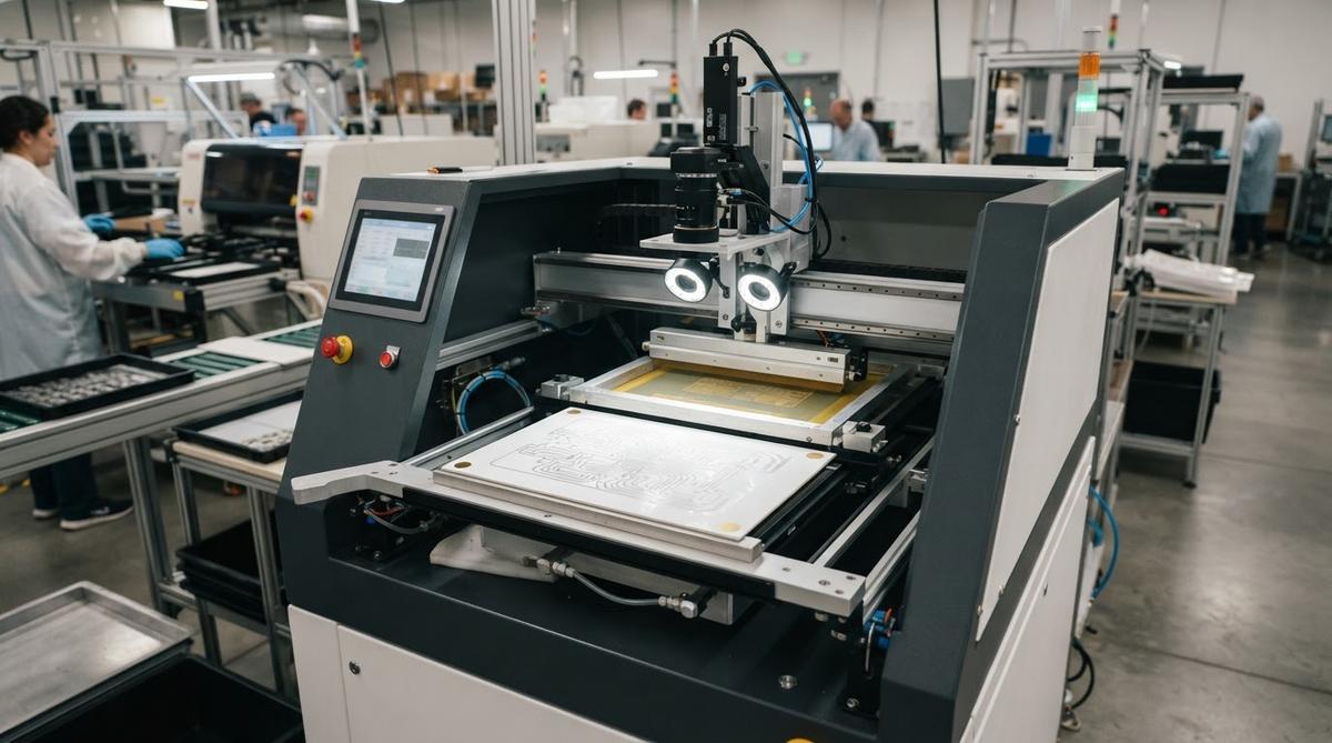
Multi-layer thick-film circuits—conductor, resistor, dielectric, then a second conductor—require printing four or more layers in registration. Modern screen printers with CCD fiducial alignment achieve ±25 µm layer-to-layer. Without vision alignment, expect ±50 µm or worse. Design rules should pad conductor-to-resistor overlap by at least 2× the registration tolerance to avoid opens.
After printing and firing, substrates can be singulated by laser scribing with positional accuracy of ±25–50 µm, so the total positional budget from print to panel breakout should be considered together.
Paste Types and Their Limits
Conductor Pastes
Silver (Ag) and gold (Au) pastes dominate. Silver is the workhorse: low cost, good conductivity (~1.5–3× bulk Ag resistivity after firing), and wide process window. Gold is used where corrosion resistance or wire-bondability matters. Copper pastes require nitrogen-atmosphere firing to prevent oxidation, adding process cost. The choice of paste directly shapes the achievable screen printing ceramic capability for a given circuit.
Resistor Pastes
Ruthenium-oxide (RuO₂) based pastes cover 1 Ω/□ to 1 MΩ/□. Fired resistance tolerance is typically ±15–20% as-printed, trimmed to ±1% by laser. Design for trimmability: leave a trim kerf area adjacent to the resistor.
Dielectric Pastes
Glass-ceramic dielectric layers provide crossover insulation and capacitor dielectrics. Typical fired thickness is 30–60 µm per layer. Breakdown voltage is 500–1000 V per layer at that thickness, per Heraeus IP9117 datasheet.
When Not to Use Screen Printing
Screen printing is the wrong process when your design requires any of the following:
- Line widths below 75 µm. Thin-film sputtering and photolithography resolve down to 10–20 µm. See thin-film capabilities on ceramic for those specs.
- Copper thickness above 100 µm. Plated or DBC copper handles high-current paths more efficiently.
- Very tight resistance tolerance (< ±0.5%) without laser trimming. Thin-film NiCr resistors offer ±0.1% as-deposited.
- Frequencies above ~20 GHz with tight impedance control. Surface roughness from screen-printed conductors (Ra 1–3 µm) increases insertion loss. Sputtered and plated conductors are smoother.
For most power electronics, LED thermal substrates, and sensor circuits operating below 10 GHz, screen printing remains the most cost-effective metallization method on ceramic. Knowing the boundaries of screen printing ceramic capability helps you avoid paying for thin-film when thick-film will do.
Frequently Asked Questions
Can screen printing deposit copper paste on ceramic?
Yes, but copper paste must be fired in a nitrogen atmosphere to prevent oxidation. This adds cost and limits the choice of co-firable resistor and dielectric pastes. Silver paste is more common for thick-film circuits for this reason.
How many print passes are needed for a 40 µm conductor?
Typically three passes with a 325-mesh screen, which deposits roughly 12–15 µm of fired silver per pass. Each pass requires a separate dry-and-fire cycle, so plan for the added process time in your lead-time estimate.
Does screen printing work on aluminum nitride (AlN)?
Yes. Standard thick-film pastes adhere well to AlN substrates, though some paste formulations require an oxide-free surface or a pre-applied adhesion layer. Confirm compatibility with the paste manufacturer’s datasheet for AlN.
What is the shelf life of thick-film paste?
Most silver and gold conductor pastes have a shelf life of 6–12 months when stored at 5–25 °C in sealed containers, per DuPont and Heraeus storage guidelines. Resistor pastes are similar. Using expired paste causes viscosity drift and inconsistent fired thickness.
Can screen-printed resistors replace SMD resistors?
For values between 10 Ω and 100 kΩ at tolerances of ±1% (after laser trimming), screen-printed thick-film resistors replace SMD parts and save board area. Below 10 Ω or above 1 MΩ, SMD components are usually more practical.
Next Step
If your design fits within the 100 µm line/space and 10–50 µm thickness window described in this screen printing ceramic capability guide, thick-film printing is likely the right metallization for your board. Review the full ceramic PCB manufacturing process to see how printing integrates with firing, via filling, and singulation. When you are ready, request a quote with your Gerber files and paste/layer stackup requirements.