DPC direct plated copper is a metallization process that deposits copper onto a ceramic substrate by vacuum sputtering a thin adhesion/seed layer, then electroplating copper to the target thickness. Typical DPC direct plated copper thickness ranges from 1 µm to 200 µm, with line/space resolution as fine as 20/20 µm at the lower end of that range. The process works on Al₂O₃, AlN, and Si₃N₄ substrates and is the go-to choice when you need finer features than thick-film printing can deliver but more current-carrying capacity than thin-film alone provides.
How the DPC Direct Plated Copper Process Builds Metal on Ceramic
The sequence matters because each step constrains what comes after it. A sputtered seed layer — typically Ti/Cu or Cr/Cu, 0.1–0.5 µm total — bonds to the ceramic surface at the atomic level. This gives DPC direct plated copper its hallmark advantage: adhesion strength of 5–8 N/mm (per IPC-TM-650 2.4.8 peel testing), far above thick-film silver or gold paste.
After sputtering, a photoresist pattern is applied and the exposed copper is electroplated to the desired thickness. Finally, the resist is stripped and the seed layer between traces is etched away. Because the copper is built up through a photolithographic mask rather than screen-printed through a mesh, feature resolution is set by the lithography, not by paste rheology.
This additive approach also means copper thickness uniformity across a panel is controlled by plating-bath chemistry and current distribution. Expect ±10% thickness uniformity on a well-managed line, tightening to ±5% on smaller substrates (≤50 mm × 50 mm).
DPC Copper Thickness Range and Achievable Tolerances
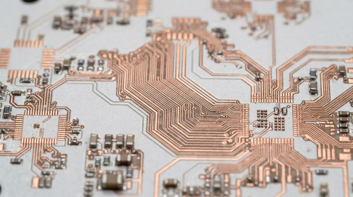
The table below summarises practical DPC direct plated copper capabilities. These figures represent what volume production lines deliver, not laboratory best-case numbers.
| Parameter | Value | Unit | Condition / Notes |
|---|---|---|---|
| Copper thickness range | 1–200 | µm | Single-layer; >100 µm may need multiple plating passes |
| Thickness tolerance | ±10% | — | Typical; ±5% achievable on small panels |
| Min line width | 20 | µm | At Cu ≤ 20 µm thickness |
| Min space | 20 | µm | At Cu ≤ 20 µm thickness |
| Min line width at 50 µm Cu | 50–75 | µm | Aspect ratio limited |
| Min line width at 100 µm Cu | 100–150 | µm | Etch undercut becomes dominant |
| Seed layer | Ti/Cu or Cr/Cu | — | 0.1–0.5 µm total |
| Peel strength | 5–8 | N/mm | Per IPC-TM-650 2.4.8 |
| Substrate compatibility | Al₂O₃ (96%, 99.6%), AlN, Si₃N₄ | — | Surface Ra ≤ 0.4 µm recommended |
| Max substrate size | Up to 190 mm × 140 mm | — | Varies by manufacturer |
Typical values for commercially available DPC processes, for comparison only. Confirm against the datasheet for your specific manufacturer and grade.
Why Copper Thickness and Line Width Are Linked in DPC
Thicker copper means wider minimum traces. This is the single most important constraint in DPC direct plated copper design. The reason is geometry: after electroplating, the seed layer between traces must be etched away. As copper gets thicker, the etchant undercuts sideways beneath the resist edge. At 20 µm copper, undercut is negligible and 20 µm lines are feasible. At 100 µm copper, undercut can reach 20–30 µm per side, forcing minimum trace widths to 100–150 µm.
A useful rule of thumb: minimum trace width ≈ 1× to 1.5× the copper thickness. If your design needs 50 µm traces carrying high current, you are limited to roughly 35–50 µm copper. If current demands push you above 100 µm copper, expect trace widths above 100 µm. For designs requiring both fine lines and thick copper on ceramic substrates, consider a two-metal-layer approach with different thicknesses on each side.
Worked Example: Trace Width for a 5 A Bus
Suppose you need a trace carrying 5 A continuous on an AlN substrate at 85 °C ambient. Using IPC-2152 as a guide (adjusted for ceramic’s superior heat spreading):
- At 50 µm Cu thickness, a 300 µm wide trace has a cross-section of 0.015 mm². Bulk copper resistivity at 85 °C is ~2.1 µΩ·cm. A 10 mm trace length gives R ≈ 14 mΩ, dissipating 0.35 W at 5 A. Acceptable for most designs.
- At 20 µm Cu thickness, the same 300 µm width gives R ≈ 35 mΩ and 0.875 W. Still manageable on ceramic, but thermal margin shrinks.
- At 100 µm Cu thickness, minimum trace width rises to ~120 µm, but R drops to ~7 mΩ and dissipation to 0.175 W. If your layout can accommodate the wider features, this is the lower-loss choice.
Enter your copper thickness, trace width, and current below to estimate resistive loss and temperature rise for a DPC trace on ceramic.
Full DPC design rules cover via sizing, pad-to-edge clearance, and registration tolerances that also shift with copper thickness.
DPC Direct Plated Copper Compared to Other Ceramic Metallization Methods
| Parameter | DPC | Thick Film (Screen Print) | DBC (Direct Bond Copper) | HTCC / LTCC |
|---|---|---|---|---|
| Cu thickness range | 1–200 µm | 5–50 µm (paste dependent) | 127–500 µm (standard foils) | 5–20 µm (co-fired conductor) |
| Min line/space | 20/20 µm | 100/100 µm | 300/300 µm | 50/50 µm (LTCC); 100/100 µm (HTCC) |
| Adhesion (peel) | 5–8 N/mm | 2–4 N/mm | >8 N/mm (eutectic bond) | 3–6 N/mm |
| Conductor material | Cu (primary); Au, Ni finish | Ag, Au, AgPd pastes | Cu | W, Mo (HTCC); Ag, Au (LTCC) |
| Multilayer capability | Single or double sided | Single or double sided | Single or double sided | 3–60+ layers |
Representative industry values. Confirm with your specific process vendor.
DPC fills the gap between thick-film’s coarse features and DBC’s minimum 127 µm foil. If you need multilayer routing, LTCC co-fired ceramic is the better path. If you need copper above 200 µm for power modules, DBC or AMB takes over.
When DPC Direct Plated Copper Is Not the Right Choice
Very high current (>50 A per trace). DPC tops out around 200 µm copper. DBC and AMB offer 300–500 µm copper with higher current-handling capacity and better thermal cycling endurance at those thicknesses.
Multilayer interconnects. DPC is inherently a single- or double-sided process. If your design needs buried vias or three or more conductor layers, HTCC or LTCC is the correct technology. See HTCC multilayer ceramic capabilities for co-fired options.
Lowest-cost high-volume LED boards. If feature sizes are above 150 µm and copper thickness is under 50 µm, screen-printed thick-film metallization costs less per panel and may be sufficient.
FR-4 is adequate. If your thermal load is under 1 W/cm² and operating temperature stays below 130 °C, standard FR-4 or metal-core PCB is cheaper and easier to source.
Frequently Asked Questions
What is the thinnest copper DPC can deposit?
DPC can plate copper as thin as 1 µm, though 3–5 µm is more common in production. Below 3 µm, the copper layer may not be continuous enough for reliable conductivity, so confirm with your fabricator’s process window.
Can DPC copper be plated on both sides of a ceramic substrate?
Yes. Double-sided DPC is standard. Each side is sputtered and plated independently, and through-substrate vias (laser-drilled or mechanically punched before metallization) connect the two sides. Via diameters as small as 100 µm are achievable on thin substrates (0.25–0.38 mm).
Does DPC direct plated copper work on aluminum nitride?
DPC is fully compatible with AlN. The Ti adhesion layer in the Ti/Cu seed stack bonds well to AlN surfaces. Surface preparation matters: AlN should be lapped to Ra ≤ 0.4 µm for best adhesion. AlN’s high thermal conductivity (170–200 W/mK) makes it a common pairing with DPC in power electronics and laser diode submounts.
How does DPC adhesion compare to DBC?
DBC copper bonds through a Cu-O eutectic at ~1065 °C, producing peel strengths above 8 N/mm. DPC achieves 5–8 N/mm via the sputtered adhesion layer. In most applications, DPC adhesion is adequate. For power modules subjected to aggressive thermal cycling (ΔT > 150 °C, thousands of cycles), DBC’s eutectic bond offers better long-term reliability.
What surface finishes can be applied over DPC copper?
Standard options include electroless nickel/immersion gold (ENIG), electrolytic nickel/gold, and electroless nickel/electroless palladium/immersion gold (ENEPIG). OSP is possible but rarely used on ceramic because ceramic boards often sit in inventory longer than OSP’s shelf life allows. Bare copper with an anti-tarnish coating works for immediate soldering.
Is DPC more expensive than thick-film printing?
Per-panel, yes. DPC requires vacuum sputtering equipment, photolithography, and electroplating — three capital-intensive steps versus one screen-print pass. Expect DPC to cost 2–4× more than thick-film for the same panel size. The premium is justified when you need finer features, tighter impedance control, or pure copper conductivity rather than silver or gold paste.