Copper plating ceramic substrates deposits conductive copper layers—typically 1–300 µm thick—onto alumina or aluminum nitride without the 1,065 °C eutectic bonding step used in DBC. The dominant production method for copper plating ceramic is Direct Plated Copper (DPC), which combines sputtered seed layers with electrolytic copper build-up to achieve fine traces (line/space down to 30/30 µm) and strong adhesion (peel strength ≥ 6 N/cm on 96% Al₂O₃). For power electronics, LED thermal management, and RF circuits, copper plating ceramic offers a practical balance of resolution, thermal performance, and cost.
Key Takeaways
- DPC copper plating ceramic achieves 1–300 µm copper thickness with line/space as fine as 30/30 µm.
- Electroless copper provides a 0.3–2 µm seed layer; electrolytic plating then builds copper to the target thickness at roughly 25 µm per hour.
- Peel strength on properly prepared 96% Al₂O₃ reaches 6–10 N/cm, per IPC-TM-650 Method 2.4.8.
- Copper plating ceramic is not a substitute for DBC when copper thickness above 300 µm or thermal cycling beyond 1,000 cycles (−55 °C to +150 °C) is required.
- Seed layer material (Ti/Cu or Cr/Cu) and substrate surface roughness (Ra 0.3–0.8 µm) are the two biggest variables affecting adhesion.
How Copper Plating Ceramic Substrates Works
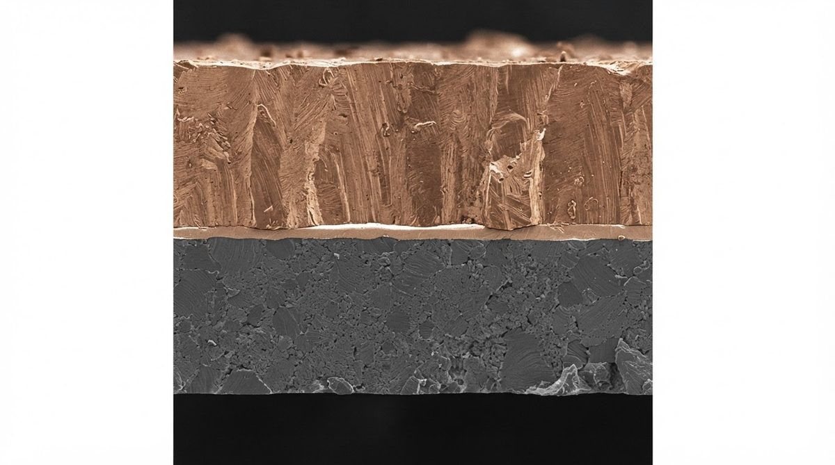
Copper does not bond spontaneously to oxide ceramics. The ceramic surface is non-conductive and chemically inert, so a multi-step ceramic metallization sequence is required before bulk copper can be deposited. The general process flow has four stages.
- Surface preparation. The substrate is cleaned ultrasonically, then plasma-treated or chemically etched to increase surface energy and micro-roughness (target Ra 0.3–0.8 µm). Higher roughness improves mechanical interlocking but degrades trace-edge definition.
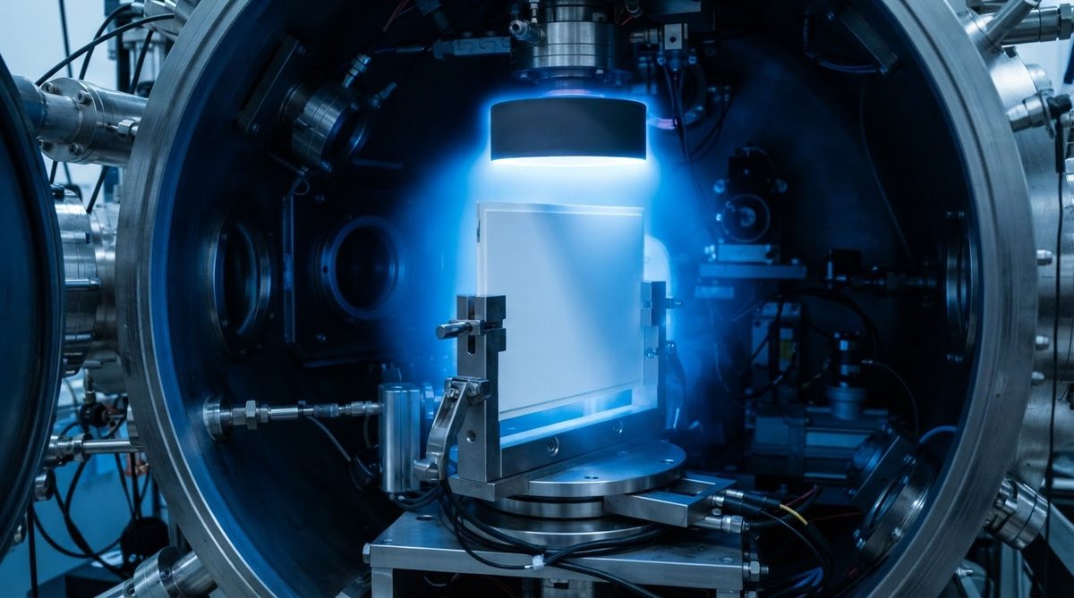
- Seed layer deposition. A thin adhesion layer (typically 20–50 nm Ti or Cr) is sputtered onto the ceramic, followed by 100–300 nm of sputtered Cu. This bilayer provides both chemical bonding to the oxide surface and electrical conductivity for subsequent electroplating.
- Pattern definition. Photoresist is applied and exposed through a mask. After developing, the open areas define the circuit pattern.
- Electrolytic copper build-up. The substrate is placed in an acid copper sulfate bath (CuSO₄ 60–80 g/L, H₂SO₄ 180–220 g/L, 20–30 °C) and plated at 2–4 A/dm². Copper grows in the resist openings at approximately 25 µm per hour. After plating, the resist is stripped and the seed layer is etched from the field areas.
This sequence is the core of the DPC (Direct Plated Copper) process. Compared with thick-film or DBC routes, DPC keeps the ceramic below 250 °C throughout, which avoids thermal stress cracking on thin substrates (< 0.38 mm).
Copper Plating Ceramic: Methods Compared
| Parameter | Electroless Cu | Electrolytic Cu (DPC) | DBC (for reference) |
|---|---|---|---|
| Typical Cu thickness | 0.3–5 µm | 1–300 µm | 127–635 µm (5–25 mil) |
| Deposition rate | 2–5 µm/hr | 20–30 µm/hr | N/A (bonded foil) |
| Min line/space | 50/50 µm | 30/30 µm | 150/150 µm |
| Peel strength (96% Al₂O₃) | 2–4 N/cm | 6–10 N/cm | ≥ 20 N/cm |
| Process temperature | 30–50 °C | 20–30 °C (bath) | 1,065 °C |
| Suitable substrates | Al₂O₃, AlN, Si₃N₄ | Al₂O₃, AlN | Al₂O₃, AlN, Si₃N₄ |
Typical values for commercially available processes, for comparison only. Confirm against the datasheet for your specific grade.
Electroless plating is primarily a seed or flash layer; it is too slow and too thin for power-carrying traces. Electrolytic plating (DPC) is the production workhorse for copper plating ceramic boards. DBC remains the choice when you need copper thicker than 300 µm or the highest possible thermal-cycle reliability. For more on thick copper options, see heavy copper on ceramic substrates.
Adhesion: What Determines Peel Strength
Adhesion failure is the primary reliability risk in copper plating ceramic assemblies. Three factors dominate.
Seed layer chemistry. A Ti adhesion layer bonds to Al₂O₃ through Ti–O chemical bonds. Cr/Cu seed layers offer similar performance but raise RoHS concerns in some markets. Per CoorsTek technical data, Ti/Cu on 96% Al₂O₃ yields 7–10 N/cm peel strength when sputtered at ≥ 0.5 Pa argon pressure.
Surface roughness. Mechanical interlocking supplements chemical bonding. An Ra of 0.4–0.6 µm is the practical sweet spot: rough enough for good adhesion, smooth enough for 50 µm line/space patterning. Lapping below Ra 0.2 µm cuts peel strength by 30–40%.
Thermal cycling stress. Copper (CTE ~17 ppm/°C) expands roughly 3× faster than Al₂O₃ (CTE ~7 ppm/°C per ASTM E228). Each thermal cycle accumulates fatigue at the Cu-ceramic interface. For plated copper at 50 µm thickness, expect reliable performance through 500+ cycles (−40 °C to +125 °C) per IPC-TM-650 2.6.7.2. Thicker plating stores more elastic energy per cycle and fails sooner.
Worked Example: Thermal Resistance of a Plated Copper Pad
A 10 × 10 mm copper pad is plated to 70 µm on a 0.635 mm thick 96% Al₂O₃ substrate. Estimate the through-substrate thermal resistance.
Copper layer: RCu = t / (k × A) = 0.00007 m / (390 W/mK × 0.0001 m²) = 0.0018 K/W.
Al₂O₃ substrate: Rsub = 0.000635 / (25 × 0.0001) = 0.254 K/W.
Total: Rth ≈ 0.256 K/W. At 5 W dissipation, ΔT ≈ 1.28 °C across the stack.
The copper layer contributes less than 1% of the total thermal resistance. Substrate material choice (Al₂O₃ vs. AlN at 170–200 W/mK) matters far more than plating thickness for thermal performance.
Design Rules for Copper-Plated Ceramic
Trace Geometry
Minimum trace width and spacing depend on copper thickness. At 20 µm Cu, 30/30 µm line/space is achievable. At 100 µm Cu, expect 75/75 µm minimum due to etch undercut during seed removal. Always specify the final copper thickness before locking trace geometry.
Via Plating
Laser-drilled vias (typically 80–200 µm diameter) in ceramic can be plated through using conformal electroless copper followed by electrolytic fill. Aspect ratios above 3:1 require pulse-reverse plating to avoid voids. Details on fill quality and inspection are covered in the via filling guide.
Edge Plating
Wrapping plated copper around substrate edges creates castellation pads for surface-mount modules. The process uses masked sputtering on routed edges followed by electrolytic build-up to 20–50 µm. Adhesion on edges is typically 60–70% of top-surface values because roughening is harder to control on a cut face. See edge plating and castellation for tolerances.
When Not to Use Copper Plating on Ceramic
You need copper thicker than 300 µm. Plating above 300 µm is slow, expensive, and prone to internal stress. DBC or AMB (Active Metal Brazing) bonds pre-rolled foil and is better suited to high-current power modules.
Your thermal cycling spec exceeds 1,000 cycles at ΔT > 150 °C. DBC and AMB copper-ceramic interfaces survive harsher cycling than plated interfaces. Si₃N₄ AMB substrates rated to 3,000+ cycles (−55 °C to +175 °C) per Kyocera SN-AMB datasheets outperform any plated solution.
Your substrate is Si₃N₄. Sputtering seed layers on silicon nitride is possible but adhesion is weaker than on alumina. Most Si₃N₄ applications use AMB instead.
FR-4 or metal-core PCB meets your requirements. If your operating temperature stays below 130 °C, your dielectric needs are standard, and your budget is tight, copper plating ceramic is over-engineering the problem.
Frequently Asked Questions
Can you plate copper directly onto AlN?
Yes. AlN requires an extra oxidation-barrier step (typically a sputtered TiN or TiW layer) between the ceramic and the Ti/Cu seed because AlN hydrolyzes in aqueous plating baths. With this barrier, peel strength on AlN reaches 5–8 N/cm.
Does plated copper survive reflow soldering on ceramic?
Plated copper with a proper seed layer survives standard Pb-free reflow profiles (peak 260 °C, per IPC J-STD-020). Apply an ENIG or ENEPIG surface finish to protect the copper from oxidation and improve solder wetting.
How thick can you plate copper on a ceramic substrate?
Practical electrolytic plating reaches 300 µm. Beyond that, internal stress causes warping and delamination risk increases sharply. For thicker copper, DBC (127–635 µm) is the standard route.
What surface finishes work on plated copper ceramic PCBs?
ENIG, ENEPIG, OSP, and immersion silver all work. ENIG (3–5 µm Ni / 0.05–0.1 µm Au per IPC-4552) is the most common for wire-bondable and solderable pads on ceramic.
Is copper plating on ceramic RoHS compliant?
Yes, provided the seed layer uses Ti/Cu rather than Cr/Cu. Hexavalent chromium (Cr⁶⁺) is restricted under RoHS Annex II. Ti/Cu seed layers contain no restricted substances.
Next Step
If you have a specific substrate, copper thickness, and trace geometry in mind, request a quote with your Gerber files or a dimensioned sketch. The fabrication team can confirm line/space limits and adhesion test data for your chosen material and thickness.