AMB active metal brazing bonds copper foil—typically 0.127 mm to 0.8 mm thick—directly to a ceramic substrate using a titanium-containing braze alloy (most commonly AgCuTi) at 780–900 °C in a vacuum furnace. The titanium reacts with the ceramic surface to form a thin intermetallic wetting layer, which allows the braze to adhere without the cuprous-oxide interlayer that DBC requires. This makes AMB active metal brazing the only practical route for bonding thick copper to silicon nitride (Si₃N₄) and the preferred method for aluminum nitride (AlN) power substrates.
Key Takeaways
- AMB active metal brazing supports copper thickness from 0.127 mm (5 mil) to 0.8 mm (31.5 mil); some suppliers offer up to 1.0 mm for custom power modules.
- Compatible substrates include Si₃N₄ (0.32 mm standard), AlN, Al₂O₃ 96%, and ZrO₂-toughened alumina (ZTA).
- Minimum trace/space for etched AMB is typically 0.3–0.5 mm, wider than DPC or thin-film processes.
- Thermal-cycle reliability on Si₃N₄ AMB substrates exceeds 3 000 cycles at −40/+150 °C per published Kyocera and Rogers data.
- AMB costs 2–5× more than DBC per unit area, driven by vacuum brazing, braze alloy cost, and longer cycle times.
How the AMB Active Metal Brazing Process Works
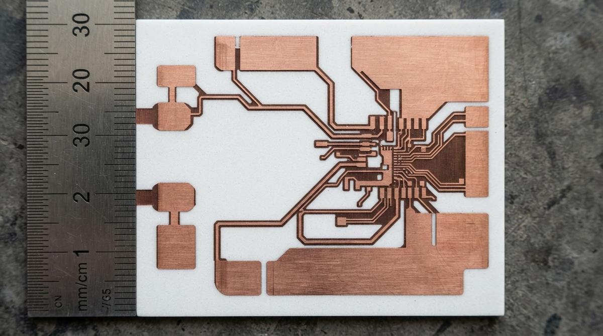
A braze foil or paste—usually Ag-Cu-Ti (often called “Cusil-ABA” or similar, ~68.8 Ag / 26.7 Cu / 4.5 Ti wt%)—is sandwiched between the copper foil and the ceramic substrate. The assembly enters a vacuum furnace at 10⁻⁴–10⁻⁵ mbar. The furnace ramps to 780–900 °C (below the Cu melting point of 1 085 °C) and holds for 10–30 minutes. During this dwell, titanium migrates to the ceramic interface and forms TiN (on AlN) or TiN + Ti₅Si₃ (on Si₃N₄), creating a chemically bonded joint.
After brazing, the copper surface is patterned by photolithography and etched to create circuit traces. Because the copper is a solid foil rather than an electroplated layer, grain structure is uniform and current-carrying capacity per unit area is high. For details on how this differs from oxide-bonded copper, see DBC direct bonded copper capabilities.
Copper Thickness and Substrate Combinations for AMB
| Substrate | Typical Thickness (mm) | Cu Foil Range (mm) | Max Recommended Cu (mm) | Notes |
|---|---|---|---|---|
| Si₃N₄ | 0.25–0.32 | 0.127–0.8 | 0.8 | Best thermal-cycle life; flexural strength >600 MPa per ASTM C1161 |
| AlN | 0.635–1.0 | 0.127–0.6 | 0.6 | High thermal conductivity (170–200 W/mK at 20 °C); more brittle than Si₃N₄ |
| Al₂O₃ 96% | 0.38–1.0 | 0.127–0.5 | 0.5 | Lowest cost; CTE mismatch limits thick-Cu reliability |
| ZTA | 0.32–0.50 | 0.127–0.6 | 0.6 | Toughness between Al₂O₃ and Si₃N₄ |
Typical values for commercially available material, for comparison only. Confirm against the datasheet for your specific grade.
Thicker copper improves current handling and thermal spreading but increases residual stress after cool-down. Si₃N₄ tolerates this stress best because its fracture toughness (6–7 MPa·√m per CoorsTek SN-1 datasheet) is roughly 2× that of AlN (2.5–3.5 MPa·√m). That is why Si₃N₄ with AMB active metal brazing dominates in EV traction inverters where 0.4–0.8 mm copper and extreme thermal cycling are the norm.
Worked Example: Current Capacity of 0.3 mm AMB Copper
A 10 mm wide, 0.3 mm thick copper trace on an AMB substrate has a cross-sectional area of 3 mm² (about 5 920 circular mils). Using the bulk resistivity of copper at 100 °C (~2.0 × 10⁻⁸ Ω·m), a 20 mm long trace has a resistance of roughly 0.133 mΩ. At 50 A DC, Joule heating is I²R = 0.33 W—manageable with even modest heatsinking. A comparable 35 µm (1 oz) FR-4 trace would need roughly 25 mm width for the same current per IPC-2221B charts, or would require multiple vias and planes.
Enter your copper dimensions, substrate material, and dissipated power below to estimate temperature rise across an AMB assembly.
AMB vs. DBC: Where Each Wins
| Parameter | AMB | DBC | Condition / Source |
|---|---|---|---|
| Bonding mechanism | Reactive braze (AgCuTi) | Cuprous oxide eutectic | — |
| Max Cu thickness | 0.8 mm (up to 1.0 mm custom) | 0.3 mm typical, 0.6 mm max | Rogers curamik, Kyocera datasheets |
| Compatible ceramics | Si₃N₄, AlN, Al₂O₃, ZTA | Al₂O₃, AlN, ZTA (not Si₃N₄) | DBC requires oxide layer |
| Thermal-cycle life (−40/+150 °C) | >3 000 cycles on Si₃N₄ | ~800–1 500 cycles on Al₂O₃ | Rogers curamik reliability data |
| Min trace/space | 0.3–0.5 mm | 0.3–0.5 mm | After etch |
| Relative cost | 2–5× DBC | 1× (baseline) | Volume-dependent |
Typical values for commercially available material, for comparison only. Confirm against the datasheet for your specific grade.
Choose DBC when Al₂O₃ meets your reliability target and cost matters. Choose AMB active metal brazing when you need Si₃N₄, copper thicker than 0.3 mm, or thermal-cycle counts above ~1 500. For finer traces below 0.3 mm, neither process is ideal; consider DPC direct plated copper or thin-film metallization instead.
Typical AMB Active Metal Brazing Design Limits
| Parameter | Value | Unit | Condition |
|---|---|---|---|
| Min trace width | 0.3–0.5 | mm | Depends on Cu thickness |
| Min space (isolation gap) | 0.3–0.5 | mm | Post-etch; wider for >3 kV isolation |
| Edge clearance (Cu to substrate edge) | ≥0.5 | mm | Prevents edge delamination |
| Substrate panel size (max) | ~190 × 140 | mm | Standard vacuum furnace tray |
| Cu thickness tolerance | ±10% | — | Foil tolerance + etch variation |
| Warp after brazing | <0.1 mm per 25 mm | — | Balanced Cu top/bottom recommended |
For detailed routing rules, pad sizing, and isolation-gap calculations, see AMB layout guidelines.
When NOT to Use AMB Active Metal Brazing
AMB is over-specified—and over-priced—for many applications. Skip it when:
- Fine-pitch circuits (<0.2 mm trace/space) are needed. DPC or thin-film processes achieve 50 µm lines routinely.
- Thermal-cycle requirements are moderate (fewer than ~1 000 cycles at −40/+125 °C). DBC on Al₂O₃ handles this at a fraction of the cost.
- Budget is the primary constraint and copper thickness below 0.3 mm is acceptable. DBC or even thick-film ceramic may suffice.
- Multi-layer routing is required. AMB is a single- or double-sided process. HTCC or LTCC offer embedded vias and internal planes.
Frequently Asked Questions
Can AMB bond copper to both sides of a ceramic substrate simultaneously?
Yes. Double-sided AMB active metal brazing is standard practice. Both copper foils are brazed in a single vacuum furnace cycle. Balancing copper thickness on both sides helps control post-braze warp.
Does AMB leave a residual braze layer between copper and ceramic?
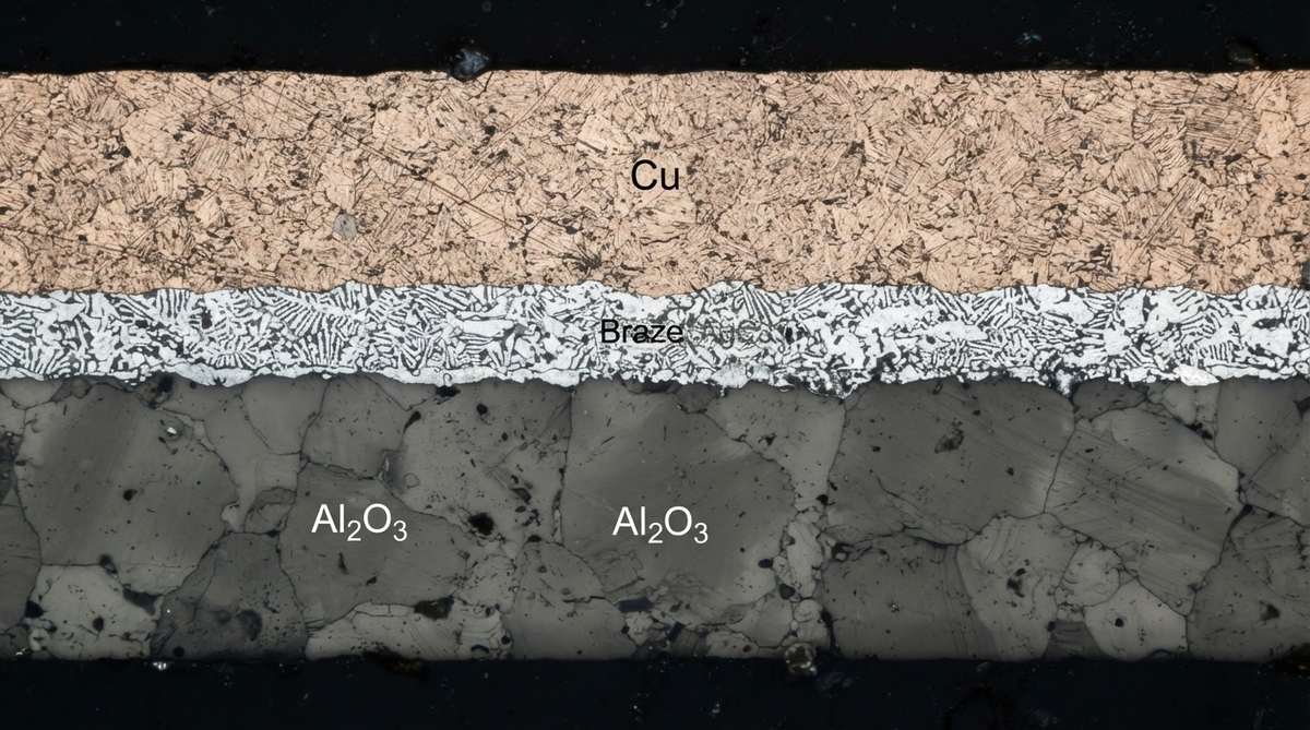
It does. The AgCuTi braze layer is typically 10–25 µm thick after bonding. This layer contributes minimal thermal resistance (on the order of 0.01–0.02 K·cm²/W) but is visible in cross-section analysis.
Is an AMB substrate suitable for wire bonding?
Yes, after surface preparation. The etched copper surface is typically plated with Ni/Au or Ni/Ag to enable reliable Al or Au wire bonding. Bare copper oxidises too quickly for consistent bond quality.
What is the maximum operating temperature for an AMB substrate?
The braze joint itself is stable to roughly 600–700 °C (well above the AgCu eutectic formation temperature of ~780 °C, because the alloy has already reacted). In practice, the copper oxidation limit (~300 °C in air without protective atmosphere) and solder-joint reliability set the ceiling, not the braze. Most power-module designs rate AMB substrates for continuous operation at 150–200 °C junction temperature.
How does AMB pricing scale with volume?
Vacuum brazing is a batch process, so per-unit cost drops significantly from prototype (single panels) to production volumes of 500+ panels. Braze alloy cost is roughly constant per area. Expect 30–50% cost reduction moving from 10-piece to 1 000-piece orders, depending on panel utilization.