A zirconia toughened ZTA PCB uses a composite ceramic substrate — Al₂O₃ blended with 10–25 wt% ZrO₂ — to achieve fracture toughness of 5–8 MPa·√m, roughly two to three times that of standard 96% alumina (3–4 MPa·√m), while retaining most of alumina’s favorable dielectric and thermal properties. For PCB applications where mechanical robustness matters as much as electrical performance, the zirconia toughened ZTA PCB fills the gap between commodity alumina and premium silicon nitride substrates.
Key Takeaways
- ZTA fracture toughness ranges from 5 to 8 MPa·√m (ASTM C1421), compared with 3–4 MPa·√m for 96% Al₂O₃ and 6–8 MPa·√m for Si₃N₄.
- Thermal conductivity of ZTA is 20–26 W/mK at 25 °C — slightly below 96% alumina’s 24–28 W/mK — because zirconia (2–3 W/mK) is a poor thermal conductor.
- ZTA is compatible with thick-film and thin-film metallization but is not processed via HTCC or LTCC co-firing routes used for multilayer ceramic packages.
- The primary cost driver is the zirconia powder and tighter sintering controls; expect 30–80% more per substrate than equivalent 96% alumina parts.
- A zirconia toughened ZTA PCB is best justified when vibration, thermal shock, or mechanical handling would crack a standard alumina board but the full cost of Si₃N₄ is not warranted.
What Is a Zirconia Toughened ZTA PCB Substrate?
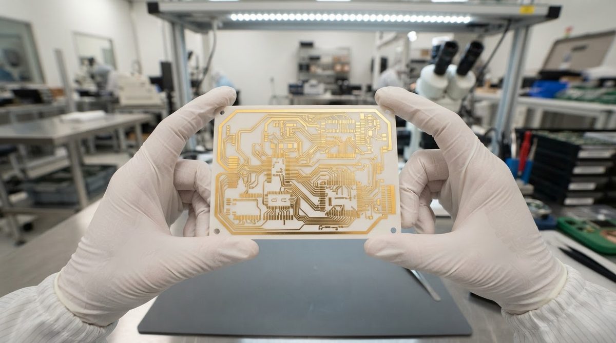
ZTA is a two-phase ceramic composite. The bulk matrix is aluminum oxide (Al₂O₃), and the toughening phase is fine-grained zirconia (ZrO₂), typically stabilized with 1.5–3 mol% yttria (Y₂O₃). When a crack propagates through the alumina matrix and reaches a zirconia grain, the grain transforms from tetragonal to monoclinic crystal structure. That transformation expands the grain by roughly 4% in volume, compressing the crack tip and absorbing energy. This mechanism — called transformation toughening — is the reason ZTA resists fracture far better than pure alumina.
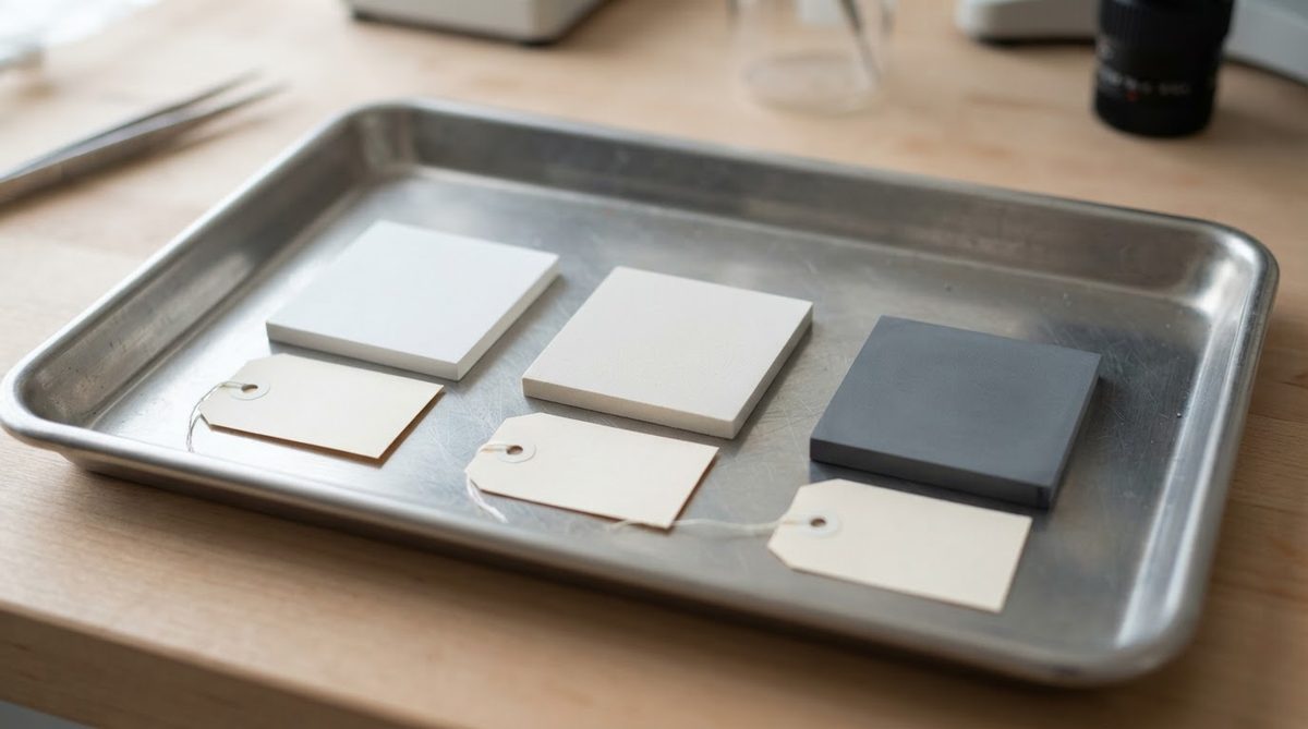
Commercially available ZTA substrates contain anywhere from 10 to 25 wt% ZrO₂. Higher zirconia content generally increases toughness but reduces thermal conductivity and raises the dielectric constant. Most PCB-grade ZTA targets 15–20 wt% ZrO₂ as a practical balance. CoorsTek markets ZTA grades under the AD-ZTA family, and Kyocera offers similar compositions; always confirm the exact zirconia fraction and stabilizer type against the supplier’s datasheet for your specific grade.
Zirconia Toughened ZTA PCB Material Properties
| Parameter | ZTA (15–20 wt% ZrO₂) | 96% Al₂O₃ | Si₃N₄ | Unit | Condition | Source |
|---|---|---|---|---|---|---|
| Fracture toughness (K_IC) | 5–8 | 3–4 | 6–8 | MPa·√m | ASTM C1421, RT | CoorsTek / Kyocera datasheets |
| Flexural strength | 500–700 | 300–380 | 700–900 | MPa | ASTM C1161, 4-pt bend, RT | CoorsTek / CeramTec datasheets |
| Thermal conductivity | 20–26 | 24–28 | 20–90 | W/mK | 25 °C | Manufacturer datasheets |
| CTE | 7.5–8.5 | 7.1–8.0 | 2.5–3.5 | ppm/°C | 25–400 °C | Manufacturer datasheets |
| Dielectric constant (ε_r) | 10–12 | 9.0–9.8 | 7–9 | — | 1 MHz, RT | Manufacturer datasheets |
| Dielectric strength | 10–15 | 10–15 | 10–17 | kV/mm | ASTM D149 | Manufacturer datasheets |
| Density | 4.0–4.3 | 3.7–3.8 | 3.2–3.3 | g/cm³ | — | Manufacturer datasheets |
Typical values for commercially available material, for comparison only. Confirm against the datasheet for your specific grade.
Two numbers stand out for designers working with a zirconia toughened ZTA PCB. First, the dielectric constant rises from roughly 9.5 (96% alumina) to 10–12 for ZTA. If you are designing controlled-impedance RF traces, that shift matters: a 50 Ω microstrip on ZTA will need a narrower trace or thicker substrate than the same line on pure alumina. Second, ZTA’s CTE (7.5–8.5 ppm/°C) is close enough to standard alumina that existing solder joint reliability data for alumina-to-copper assemblies largely transfers.
Enter your substrate dimensions, thickness, and dissipated power below to estimate the junction-to-case temperature rise for a ZTA or alumina substrate.
How ZTA Substrates Are Metallized
ZTA substrates are sintered at 1 500–1 600 °C and supplied as finished blanks. Metallization is applied after sintering, using the same post-fire methods used for standard alumina. Compatible processes include:
- Thick-film screen printing — Ag, Au, or Ag/Pd pastes fired at 850 °C. The most common route for hybrid circuits and power modules on ZTA.
- Thin-film sputtering — Ti/Pt/Au or Cr/Ni/Au stacks for fine-line RF and sensor circuits. Adhesion to ZTA is comparable to adhesion on 96% alumina when the surface is lapped to Ra ≤ 0.4 µm.
- Active metal brazing (AMB) — TiAg-Cu or similar active brazes can bond thick copper (0.3 mm) directly to ZTA for power electronics. AMB on ZTA is a niche but growing application.
ZTA is not compatible with HTCC or LTCC co-firing. Those processes require green-state tape casting of the ceramic itself, and ZTA’s two-phase microstructure does not survive the tape-casting and co-sintering steps used for multilayer packages. If you need a multilayer ceramic, standard alumina (HTCC) or glass-ceramic (LTCC) is the correct choice. For a broader comparison of ceramic PCB material options, see our material selection guide.
Substrates can also be laser-cut into custom shapes after sintering, though ZTA’s higher toughness means slightly higher laser energy is needed compared with pure alumina, and edge chipping is actually less of a concern.
Worked Example: Thermal Resistance on a ZTA PCB
Suppose you mount a 10 W power transistor on a 25 × 25 mm ZTA substrate, 0.635 mm thick. Thermal conductivity is 22 W/mK (mid-range for ZTA). The conduction thermal resistance through the substrate is:
R_th = t / (k × A) = 0.000635 / (22 × 0.000625) = 0.046 °C/W
At 10 W dissipation, the temperature drop across the substrate is about 0.46 °C. For comparison, the same geometry in 96% alumina at 26 W/mK gives 0.039 °C/W, and in FR-4 (0.3 W/mK) gives 3.39 °C/W. The thermal penalty of ZTA versus pure alumina is small — roughly 0.07 °C at 10 W — and is usually dwarfed by the solder-joint and heatsink interface resistances in a real assembly.
Where Zirconia Toughened ZTA PCBs Make Sense
A zirconia toughened ZTA PCB earns its cost premium in a narrow but well-defined set of applications:
- Downhole and mining electronics — Boards see sustained vibration and mechanical shock. Standard alumina cracks; ZTA survives.
- Automotive power modules under thermal cycling — ZTA’s higher flexural strength extends crack-initiation life under –40 to +150 °C cycling compared with 96% alumina. The CTE match to copper is similar, so solder joint fatigue is not penalized.
- Aerospace and defense sensor substrates — Where a cracked substrate means a mission failure and Si₃N₄ cost is not justified.
- Medical implant electronics — Biocompatible, hermetic, and resistant to handling damage during assembly.
If your application also demands very high thermal conductivity (>100 W/mK), ZTA is not the answer. Look at ceramic thermal management substrates such as aluminum nitride (AlN), which offer 170–200 W/mK at the cost of lower fracture toughness (2.5–3.5 MPa·√m).
ZTA vs. 96% Alumina vs. Si₃N₄: A Decision Framework
| Decision factor | 96% Al₂O₃ | ZTA | Si₃N₄ |
|---|---|---|---|
| Fracture toughness | 3–4 MPa·√m | 5–8 MPa·√m | 6–8 MPa·√m |
| Thermal conductivity | 24–28 W/mK | 20–26 W/mK | 20–90 W/mK |
| CTE match to copper | Good (7–8 vs 17 ppm/°C) | Good (7.5–8.5 ppm/°C) | Poor (2.5–3.5 ppm/°C) |
| Relative substrate cost | 1× | 1.3–1.8× | 3–6× |
| Multilayer (HTCC/LTCC) | Yes (HTCC) | No | No |
| Best for | General ceramic PCB use | Vibration/shock environments | Extreme thermal cycling, EV inverters |
Typical values for commercially available material, for comparison only. Confirm against the datasheet for your specific grade.
If your board sees no unusual mechanical stress and cost is a priority, 96% alumina PCBs remain the default ceramic substrate. If you need the absolute highest thermal-cycling reliability for thick-copper power modules, Si₃N₄ is the proven choice despite its cost. The zirconia toughened ZTA PCB sits between them: tougher than alumina, cheaper than silicon nitride, and compatible with standard alumina metallization processes.
When Not to Use ZTA
ZTA is not the right substrate in several common scenarios:
- Cost-sensitive, high-volume consumer electronics — Standard 96% alumina or even metal-core PCBs (MCPCBs) will do the job at a fraction of the price.
- Multilayer ceramic packages — ZTA cannot be co-fired. Use HTCC alumina or LTCC glass-ceramic.
- High-frequency RF above 10 GHz — ZTA’s dielectric constant (10–12) and higher dielectric loss tangent compared with 99.6% alumina make it a poor choice for millimeter-wave circuits. Consider 99.6% alumina substrates or quartz instead.
- Applications demanding thermal conductivity above 30 W/mK — AlN or high-grade Si₃N₄ is the better path.
- Cryogenic environments — ZTA’s transformation-toughening mechanism can become less effective below –100 °C as the tetragonal phase stabilizes. If your board operates at cryogenic temperatures, review ceramic PCBs for cryogenic use for material-specific guidance.
Sourcing ZTA Substrates and PCBs
ZTA substrates are produced by specialty ceramic manufacturers such as CoorsTek, Kyocera, and CeramTec. When sourcing, specify the zirconia weight fraction, stabilizer type (yttria vs. ceria), surface finish (as-fired vs. lapped), and dimensional tolerances. A common mistake is specifying “ZTA” without the ZrO₂ fraction; a 10 wt% ZTA and a 25 wt% ZTA have meaningfully different properties.
For metallized ZTA boards, provide the ceramic PCB manufacturing process details — paste chemistry, firing profile, copper thickness — alongside the substrate spec. Mismatched paste and substrate can cause delamination or blister defects after firing.
After metallization, boards should pass reliability screening and testing appropriate to the end application, including thermal shock cycling per MIL-STD-883 if the board targets aerospace or defense use.
Frequently Asked Questions
Can you solder to a ZTA ceramic PCB?
Yes. ZTA accepts the same thick-film and thin-film metallization as standard alumina, so standard soldering (SnAgCu, AuSn, or high-temperature Pb-based alloys) works without modification. Surface finish options include ENIG, ENEPIG, and bare gold pads.
Does a zirconia toughened ZTA PCB cost more than standard alumina?
ZTA substrates typically cost 30–80% more than equivalent 96% alumina parts. The premium comes from higher-purity zirconia powder and tighter sintering temperature control needed to achieve the correct tetragonal ZrO₂ phase.
Is ZTA available as a DBC substrate?
Direct bond copper (DBC) on ZTA is technically feasible because ZTA forms a copper-aluminate bond layer similar to pure alumina. However, DBC on ZTA is far less common commercially than DBC on standard Al₂O₃ or AlN. AMB (active metal brazing) is the more established thick-copper bonding method for ZTA substrates.
How does a ZTA PCB perform under thermal cycling?
ZTA’s higher fracture toughness delays crack initiation under repeated thermal stress. Published studies (e.g., Choi & Bansal, J. Am. Ceram. Soc., 2005) show ZTA surviving 2–3× more thermal cycles than 96% alumina before substrate cracking in –55 to +150 °C accelerated tests. Solder joint reliability is comparable because ZTA’s CTE is close to alumina’s.
What surface finish does a ZTA substrate need before metallization?
For thick-film printing, an as-fired surface (Ra 0.5–1.0 µm) is adequate. For thin-film sputtering, lapping to Ra ≤ 0.4 µm is recommended to ensure uniform adhesion of the seed layer. Polished surfaces (Ra < 0.05 µm) are used for demanding sensor or MEMS applications.
Next Step
If you are evaluating a zirconia toughened ZTA PCB against standard alumina or silicon nitride for a specific board, start by reviewing the full ceramic substrate material comparison to narrow the field. When you are ready to get pricing on ZTA or any other ceramic substrate, request a quote through our instant quote page with your substrate dimensions, zirconia fraction, and metallization requirements.